SNVSBA5C December   2019  – May 2024 LP8866-Q1

PRODUCTION DATA  

  1.   1
  2. Features
  3. Applications
  4. Description
  5. Pin Configuration and Functions
  6. Specifications
    1. 5.1 Absolute Maximum Ratings
    2. 5.2 ESD Ratings
    3. 5.3 Recommended Operating Conditions
    4. 5.4 Thermal Information
    5. 5.5 Electrical Characteristics
    6. 5.6 Logic Interface Characteristics
    7. 5.7 Timing Requirements for I2C Interface
    8.     14
    9. 5.8 Typical Characteristics
  7. Detailed Description
    1. 6.1 Overview
    2. 6.2 Functional Block Diagram
    3. 6.3 Feature Description
      1. 6.3.1 Control Interface
      2. 6.3.2 Function Setting
      3. 6.3.3 Device Supply (VDD)
      4. 6.3.4 Enable (EN)
      5. 6.3.5 Charge Pump
      6. 6.3.6 Boost Controller
        1. 6.3.6.1 Boost Cycle-by-Cycle Current Limit
        2. 6.3.6.2 Controller Min On/Off Time
        3. 6.3.6.3 Boost Adaptive Voltage Control
          1. 6.3.6.3.1 FB Divider Using Two-Resistor Method
          2. 6.3.6.3.2 FB Divider Using Three-Resistor Method
          3. 6.3.6.3.3 FB Divider Using External Compensation
        4. 6.3.6.4 Boost Sync and Spread Spectrum
        5. 6.3.6.5 Boost Output Discharge
        6. 6.3.6.6 Light Load Mode
      7. 6.3.7 LED Current Sinks
        1. 6.3.7.1 LED Output Current Setting
        2. 6.3.7.2 LED Output String Configuration
        3. 6.3.7.3 LED Output PWM Clock Generation
      8. 6.3.8 Brightness Control
        1. 6.3.8.1 Brightness Control Signal Path
        2. 6.3.8.2 Dimming Mode
        3. 6.3.8.3 LED Dimming Frequency
        4. 6.3.8.4 Phase-Shift PWM Mode
        5. 6.3.8.5 Hybrid Mode
        6. 6.3.8.6 Direct PWM Mode
        7. 6.3.8.7 Sloper
        8. 6.3.8.8 PWM Detector Hysteresis
        9. 6.3.8.9 Dither
      9. 6.3.9 Protection and Fault Detections
        1. 6.3.9.1 Supply Faults
          1. 6.3.9.1.1 VIN Undervoltage Faults (VINUVLO)
          2. 6.3.9.1.2 VIN Overvoltage Faults (VINOVP)
          3. 6.3.9.1.3 VDD Undervoltage Faults (VDDUVLO)
          4. 6.3.9.1.4 VIN OCP Faults (VINOCP)
            1. 6.3.9.1.4.1 VIN OCP Current Limit vs. Boost Cycle-by-Cycle Current Limit
          5. 6.3.9.1.5 Charge Pump Faults (CPCAP, CP)
          6. 6.3.9.1.6 CRC Error Faults (CRCERR)
        2. 6.3.9.2 Boost Faults
          1. 6.3.9.2.1 Boost Overvoltage Faults (BSTOVPL, BSTOVPH)
          2. 6.3.9.2.2 Boost Overcurrent Faults (BSTOCP)
          3. 6.3.9.2.3 LEDSET Resistor Missing Faults (LEDSET)
          4. 6.3.9.2.4 MODE Resistor Missing Faults (MODESEL)
          5. 6.3.9.2.5 FSET Resistor Missing Faults (FSET)
          6. 6.3.9.2.6 ISET Resistor Out of Range Faults (ISET)
          7. 6.3.9.2.7 Thermal Shutdown Faults (TSD)
        3. 6.3.9.3 LED Faults
          1. 6.3.9.3.1 Open LED Faults (OPEN_LED)
          2. 6.3.9.3.2 Short LED Faults (SHORT_LED)
          3. 6.3.9.3.3 LED Short to GND Faults (GND_LED)
          4. 6.3.9.3.4 Invalid LED String Faults (INVSTRING)
          5. 6.3.9.3.5 I2C Timeout Faults
        4. 6.3.9.4 Overview of the Fault and Protection Schemes
    4. 6.4 Device Functional Modes
      1. 6.4.1  State Diagram
      2. 6.4.2  Shutdown
      3. 6.4.3  Device Initialization
      4. 6.4.4  Standby Mode
      5. 6.4.5  Power-line FET Soft Start
      6. 6.4.6  Boost Start-Up
      7. 6.4.7  Normal Mode
      8. 6.4.8  Fault Recovery
      9. 6.4.9  Latch Fault
      10. 6.4.10 Start-Up Sequence
    5. 6.5 Programming
      1. 6.5.1 I2C-Compatible Interface
      2. 6.5.2 Programming Examples
        1. 6.5.2.1 General Configuration Registers
        2. 6.5.2.2 Clearing Fault Interrupts
        3. 6.5.2.3 Disabling Fault Interrupts
        4. 6.5.2.4 Diagnostic Registers
  8. Register Maps
    1. 7.1 FullMap Registers
  9. Application and Implementation
    1. 8.1 Application Information
    2. 8.2 Typical Applications
      1. 8.2.1 Full Feature Application for Display Backlight
        1. 8.2.1.1 Design Requirements
        2. 8.2.1.2 Detailed Design Procedure
          1. 8.2.1.2.1  Inductor Selection
          2. 8.2.1.2.2  Output Capacitor Selection
          3. 8.2.1.2.3  Input Capacitor Selection
          4. 8.2.1.2.4  Charge Pump Output Capacitor
          5. 8.2.1.2.5  Charge Pump Flying Capacitor
          6. 8.2.1.2.6  Output Diode
          7. 8.2.1.2.7  Switching FET
          8. 8.2.1.2.8  Boost Sense Resistor
          9. 8.2.1.2.9  Power-Line FET
          10. 8.2.1.2.10 Input Current Sense Resistor
          11. 8.2.1.2.11 Feedback Resistor Divider
          12. 8.2.1.2.12 Critical Components for Design
        3. 8.2.1.3 Application Curves
      2. 8.2.2 Application with Basic/Minimal Operation
        1. 8.2.2.1 Design Requirements
        2. 8.2.2.2 Detailed Design Procedure
        3. 8.2.2.3 Application Curves
      3. 8.2.3 SEPIC Mode Application
        1. 8.2.3.1 Design Requirements
        2. 8.2.3.2 Detailed Design Procedure
          1. 8.2.3.2.1  Inductor Selection
          2. 8.2.3.2.2  Coupling Capacitor Selection
          3. 8.2.3.2.3  Output Capacitor Selection
          4. 8.2.3.2.4  Input Capacitor Selection
          5. 8.2.3.2.5  Charge Pump Output Capacitor
          6. 8.2.3.2.6  Charge Pump Flying Capacitor
          7. 8.2.3.2.7  Switching FET
          8. 8.2.3.2.8  Output Diode
          9. 8.2.3.2.9  Switching Sense Resistor
          10. 8.2.3.2.10 Power-Line FET
          11. 8.2.3.2.11 Input Current Sense Resistor
          12. 8.2.3.2.12 Feedback Resistor Divider
          13. 8.2.3.2.13 Critical Components for Design
        3. 8.2.3.3 Application Curves
    3. 8.3 Power Supply Recommendations
    4. 8.4 Layout
      1. 8.4.1 Layout Guidelines
      2. 8.4.2 Layout Example
  10. Device and Documentation Support
    1. 9.1 Device Support
      1. 9.1.1 Third-Party Products Disclaimer
    2. 9.2 Receiving Notification of Documentation Updates
    3. 9.3 Support Resources
    4. 9.4 Trademarks
    5. 9.5 Electrostatic Discharge Caution
    6. 9.6 Glossary
  11. 10Revision History
  12. 11Mechanical, Packaging, and Orderable Information

Package Options

Mechanical Data (Package|Pins)
Thermal pad, mechanical data (Package|Pins)
Open LED Faults (OPEN_LED)

During normal boost operation, boost voltage is raised if any of the used LED outputs falls below the LED_DRV_HEADROOM threshold level. Open LED fault is detected if boost output voltage has reached the maximum and at least one LED output is still below the threshold. The open string is then disconnected from the boost adaptive control loop and its output is disabled. Any LED fault sets the status bit LED_STATUS and an interrupt is generated unless LED interrupt is disabled. The detail of open LED faults can be read from bits OPEN_LED and LEDx_FAULT (x = 1...6). These bits maintain their value until device power-down. But the LED_STATUS bit could be cleared by the interrupt clearing procedure. If a new LED fault is detected, LED_STATUS is set and an interrupt generated again.
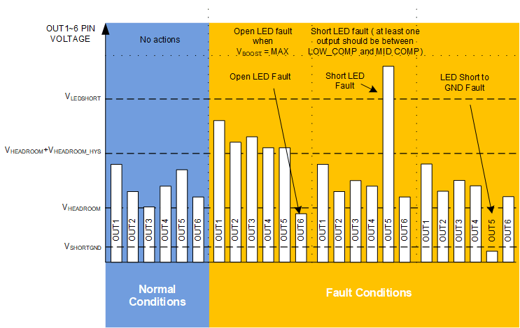
LP8866-Q1 LED Open and Short Detection
                    Logic Figure 6-18 LED Open and Short Detection Logic