SNVSBA5C December 2019 – May 2024 LP8866-Q1
PRODUCTION DATA
- 1
- 1 Features
- 2 Applications
- 3 Description
- 4 Pin Configuration and Functions
- 5 Specifications
-
6 Detailed Description
- 6.1 Overview
- 6.2 Functional Block Diagram
- 6.3
Feature Description
- 6.3.1 Control Interface
- 6.3.2 Function Setting
- 6.3.3 Device Supply (VDD)
- 6.3.4 Enable (EN)
- 6.3.5 Charge Pump
- 6.3.6 Boost Controller
- 6.3.7 LED Current Sinks
- 6.3.8 Brightness Control
- 6.3.9
Protection and Fault Detections
- 6.3.9.1 Supply Faults
- 6.3.9.2
Boost Faults
- 6.3.9.2.1 Boost Overvoltage Faults (BSTOVPL, BSTOVPH)
- 6.3.9.2.2 Boost Overcurrent Faults (BSTOCP)
- 6.3.9.2.3 LEDSET Resistor Missing Faults (LEDSET)
- 6.3.9.2.4 MODE Resistor Missing Faults (MODESEL)
- 6.3.9.2.5 FSET Resistor Missing Faults (FSET)
- 6.3.9.2.6 ISET Resistor Out of Range Faults (ISET)
- 6.3.9.2.7 Thermal Shutdown Faults (TSD)
- 6.3.9.3 LED Faults
- 6.3.9.4 Overview of the Fault and Protection Schemes
- 6.4 Device Functional Modes
- 6.5 Programming
- 7 Register Maps
-
8 Application and Implementation
- 8.1 Application Information
- 8.2
Typical Applications
- 8.2.1
Full Feature Application for Display Backlight
- 8.2.1.1 Design Requirements
- 8.2.1.2
Detailed Design Procedure
- 8.2.1.2.1 Inductor Selection
- 8.2.1.2.2 Output Capacitor Selection
- 8.2.1.2.3 Input Capacitor Selection
- 8.2.1.2.4 Charge Pump Output Capacitor
- 8.2.1.2.5 Charge Pump Flying Capacitor
- 8.2.1.2.6 Output Diode
- 8.2.1.2.7 Switching FET
- 8.2.1.2.8 Boost Sense Resistor
- 8.2.1.2.9 Power-Line FET
- 8.2.1.2.10 Input Current Sense Resistor
- 8.2.1.2.11 Feedback Resistor Divider
- 8.2.1.2.12 Critical Components for Design
- 8.2.1.3 Application Curves
- 8.2.2 Application with Basic/Minimal Operation
- 8.2.3
SEPIC Mode Application
- 8.2.3.1 Design Requirements
- 8.2.3.2
Detailed Design Procedure
- 8.2.3.2.1 Inductor Selection
- 8.2.3.2.2 Coupling Capacitor Selection
- 8.2.3.2.3 Output Capacitor Selection
- 8.2.3.2.4 Input Capacitor Selection
- 8.2.3.2.5 Charge Pump Output Capacitor
- 8.2.3.2.6 Charge Pump Flying Capacitor
- 8.2.3.2.7 Switching FET
- 8.2.3.2.8 Output Diode
- 8.2.3.2.9 Switching Sense Resistor
- 8.2.3.2.10 Power-Line FET
- 8.2.3.2.11 Input Current Sense Resistor
- 8.2.3.2.12 Feedback Resistor Divider
- 8.2.3.2.13 Critical Components for Design
- 8.2.3.3 Application Curves
- 8.2.1
Full Feature Application for Display Backlight
- 8.3 Power Supply Recommendations
- 8.4 Layout
- 9 Device and Documentation Support
- 10Revision History
- 11Mechanical, Packaging, and Orderable Information
4 Pin Configuration and Functions
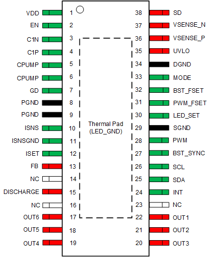
 Figure 4-1 DCP Package38-Pin HTSSOPTop View
Product preview
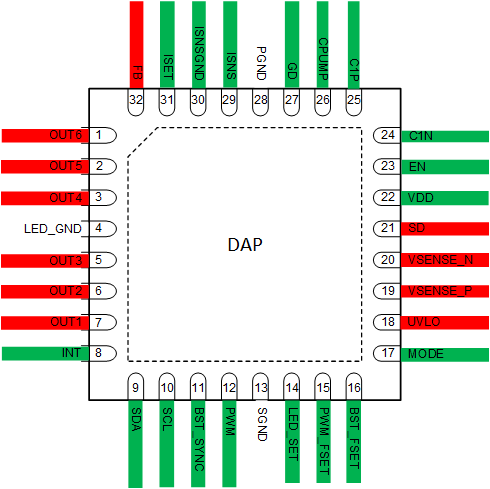
Figure 4-2 RHB Package32-PIN QFNTop ViewTable 4-1 HTTSOP Pin Functions
| PIN | TYPE | DESCRIPTION | |
|---|---|---|---|
| NO. | NAME | ||
| 1 | VDD | Power | Power supply input for internal analog and digital circuit. Connect a 10μF capacitor between the VDD pin to GND. |
| 2 | EN | Analog | Enable input. |
| 3 | C1N | Analog | Negative input for charge pump flying capacitor. If feature not used leave this pin floating. |
| 4 | C1P | Analog | Positive input for charge pump flying capacitor. If feature not used leave this pin floating. |
| 5 | CPUMP | Power | Charge pump output pin. Connect to VDD if charge pump is not used. A 4.7µF decoupling capacitor is recommended on CPUMP pin. |
| 6 | CPUMP | Power | Charge pump output pin. Always connects with pin 5. |
| 7 | GD | Analog | Gate driver output for external N-FET. |
| 8 | PGND | GND | Power ground. |
| 9 | PGND | GND | Power ground. |
| 10 | ISNS | Analog | Boost current sense pin. |
| 11 | ISNSGND | GND | Current sense resistor GND. |
| 12 | ISET | Analog | LED full-scale current setup through external resistor. |
| 13 | FB | Analog | Boost feedback input. |
| 14 | NC | N/A | No connect - Leave floating. |
| 15 | DISCHARGE | Analog | Boost output voltage discharge pin. Connect to Boost output. |
| 16 | NC | N/A | No connect - Leave floating. |
| 17 | OUT6 | Analog | LED current sink output. If unused tie to ground.. |
| 18 | OUT5 | Analog | LED current sink output. If unused tie to ground.. |
| 19 | OUT4 | Analog | LED current sink output. If unused tie to ground. |
| 20 | OUT3 | Analog | LED current sink output. If unused tie to ground. |
| 21 | OUT2 | Analog | LED current sink output. If unused tie to ground. |
| 22 | OUT1 | Analog | LED current sink output. If unused tie to ground. |
| 23 | NC | N/A | No connect - Leave floating. |
| 24 | INT | Analog | Device fault interrupt output, open drain. A 10kΩ pullup resistor is recommended. |
| 25 | SDA | Analog | SDA for I2C interface. A 10kΩ pullup resistor is recommended. |
| 26 | SCL | Analog | SCL for I2C interface. A 10kΩ pullup resistor is recommended. |
| 27 | BST_SYNC | Analog | Input for synchronizing boost. When synchronization is not used, connect this pin to ground to disable spread spectrum or to VDD to enable spread spectrum. |
| 28 | PWM | Analog | PWM input for brightness control. Tie to GND if unused. |
| 29 | SGND | GND | Signal ground. |
| 30 | LED_SET | Analog | LED string configuration through external resistor. Do not leave floating. |
| 31 | PWM_FSET | Analog | LED dimming frequency setup through external resistor. Do not leave floating. |
| 32 | BST_FSET | Analog | Boost switching frequency setup through external resistor. Do not leave floating. |
| 33 | MODE | Analog | Dimming mode setup through external resistor. Do not leave floating. |
| 34 | DGND | GND | Digital ground. |
| 35 | UVLO | Analog | Input voltage sense for programming input UVLO threshold through external resistor to VIN. |
| 36 | VSENSE_P | Analog | Pin for input voltage detection for OVP protection and positive input for input current sense. |
| 37 | VSENSE_N | Analog | Negative input for input current sense. If input current sense is not used, please tie to VSENSE_P pin. |
| 38 | SD | Analog | Power line FET control. Open Drain output. If unused, leave this pin floating. |
| DAP | LED_GND | GND | LED ground connection. |
Table 4-2 QFN Pin Functions
| PIN | TYPE | DESCRIPTION | |
|---|---|---|---|
| NO. | NAME | ||
| 1 | OUT6 | Analog | LED current sink output. If unused tie to ground.. |
| 2 | OUT5 | Analog | LED current sink output. If unused tie to ground.. |
| 3 | OUT4 | Analog | LED current sink output. If unused tie to ground. |
| 4 | LED_GND | GND | LED ground connection. |
| 5 | OUT3 | Analog | LED current sink output. If unused tie to ground. |
| 6 | OUT2 | Analog | LED current sink output. If unused tie to ground. |
| 7 | OUT1 | Analog | LED current sink output. If unused tie to ground. |
| 8 | INT | Analog | Device fault interrupt output, open drain. A 10kΩ pullup resistor is recommended. |
| 9 | SDA | Analog | SDA for I2C interface. A 10kΩ pullup resistor is recommended. |
| 10 | SCL | Analog | SCL for I2C interface. A 10kΩ pullup resistor is recommended. |
| 11 | BST_SYNC | Analog | Input for synchronizing boost. When synchronization is not used, connect this pin to ground to disable spread spectrum or to VDD to enable spread spectrum. |
| 12 | PWM | Analog | PWM input for brightness control. Tie to GND if unused. |
| 13 | SGND | GND | Signal ground. |
| 14 | LED_SET | Analog | LED string configuration through external resistor. Do not leave floating. |
| 15 | PWM_FSET | Analog | LED dimming frequency setup through external resistor. Do not leave floating. |
| 16 | BST_FSET | Analog | Boost switching frequency setup through external resistor. Do not leave floating. |
| 17 | MODE | Analog | Dimming mode setup through external resistor. Do not leave floating. |
| 18 | UVLO | Analog | Input voltage sense for programming input UVLO threshold through external resistor to VIN. |
| 19 | VSENSE_P | Analog | Pin for input voltage detection for OVP protection and positive input for input current sense. |
| 20 | VSENSE_N | Analog | Negative input for input current sense. If input current sense is not used, please tie to VSENSE_P pin. |
| 21 | SD | Analog | Power line FET control. Open Drain output. If unused, leave this pin floating. |
| 22 | VDD | Power | Power supply input for internal analog and digital circuit. Connect a 10μF capacitor between the VDD pin to GND |
| 23 | EN | Analog | Enable input. |
| 24 | C1N | Analog | Negative input for charge pump flying capacitor. If feature not used leave this pin floating. |
| 25 | C1P | Analog | Positive input for charge pump flying capacitor. If feature not used leave this pin floating. |
| 26 | CPUMP | Power | Charge pump output pin. Connect to VDD if charge pump is not used. A 4.7µF decoupling capacitor is recommended on CPUMP pin. |
| 27 | GD | Analog | Gate driver output for external N-FET. |
| 28 | PGND | GND | Power ground. |
| 29 | ISNS | Analog | Boost current sense pin. |
| 30 | ISNSGND | GND | Current sense resistor GND. |
| 31 | ISET | Analog | LED full-scale current setup through external resistor. |
| 32 | FB | Analog | Boost feedback input. |
| DAP | LED_GND | GND | LED ground connection. |