SNVS542E May 2008 – June 2016 LP8900
PRODUCTION DATA.
- 1 Features
- 2 Applications
- 3 Description
- 4 Revision History
- 5 Default Device Options
- 6 Pin Configuration and Functions
- 7 Specifications
- 8 Detailed Description
- 9 Application and Implementation
- 10Power Supply Recommendations
- 11Layout
- 12Device and Documentation Support
- 13Mechanical, Packaging, and Orderable Information
Package Options
Mechanical Data (Package|Pins)
- YZR|6
Thermal pad, mechanical data (Package|Pins)
Orderable Information
7 Specifications
7.1 Absolute Maximum Ratings
over operating free-air temperature range (unless otherwise noted)(1)(2)| MIN | MAX | UNIT | ||
|---|---|---|---|---|
| IN, OUT pins: Voltage to GND | –0.3 | 6.5 | V | |
| EN pin: Voltage to GND | –0.3 to (VIN + 0.3V) | 6.5 | °C | |
| Continuous power dissipation(3) | Internally limited | |||
| Junction temperature | 150 | °C | ||
| Storage temperature, Tstg | –65 | 150 | °C | |
(1) Stresses beyond those listed under Absolute Maximum Ratings may cause permanent damage to the device. These are stress ratings only, which do not imply functional operation of the device at these or any other conditions beyond those indicated under Recommended Operating Conditions. Exposure to absolute-maximum-rated conditions for extended periods may affect device reliability.
(2) All voltages are with respect to the potential at the GND pin.
(3) Internal thermal shutdown circuitry protects the device from permanent damage.
7.2 ESD Ratings
| VALUE | UNIT | |||
|---|---|---|---|---|
| V(ESD) | Electrostatic discharge | Human-body model (HBM), per ANSI/ESDA/JEDEC JS-001(1) | ±2000 | V |
| Charged-device model (CDM), per JEDEC specification JESD22-C101(2) | ±200 | |||
(1) JEDEC document JEP155 states that 500-V HBM allows safe manufacturing with a standard ESD control process.
(2) JEDEC document JEP157 states that 250-V CDM allows safe manufacturing with a standard ESD control process.
7.3 Recommended Operating Conditions
over operating free-air temperature range (unless otherwise noted)(1)| MIN | NOM | MAX | UNIT | ||
|---|---|---|---|---|---|
| Input voltage | 1.8 | 5.5 | V | ||
| Recommended load current per channel | 200 | mA | |||
| Junction temperature, TJ | –40 | 125 | °C | ||
| Ambient temperature, TA(2) | –40 | 85 | °C | ||
(1) Stresses beyond those listed under Absolute Maximum Ratings may cause permanent damage to the device. These are stress ratings only, which do not imply functional operation of the device at these or any other conditions beyond those indicated under Recommended Operating Conditions. Exposure to absolute-maximum-rated conditions for extended periods may affect device reliability.
(2) The maximum ambient temperature (TA(MAX)) is dependant on the maximum operating junction temperature (TJ(MAX-OP) = 125°C), the maximum power dissipation of the device in the application (PD(MAX)), and the junction to ambient thermal resistance of the part / package in the application (RθJA), as given by: TA(MAX) = TJ(MAX-OP) – (RθJA × PD(MAX)).
7.4 Thermal Information
| THERMAL METRIC(1) | LP8900 | UNIT | |
|---|---|---|---|
| YZR (DSBGA) | |||
| 6 PINS | |||
| RθJA | Junction-to-ambient thermal resistance | 140.0 | °C/W |
| RθJC(top) | Junction-to-case (top) thermal resistance | 1.0 | °C/W |
| RθJB | Junction-to-board thermal resistance | 26.0 | °C/W |
| ψJT | Junction-to-top characterization parameter | 0.3 | °C/W |
| ψJB | Junction-to-board characterization parameter | 26.0 | °C/W |
(1) For more information about traditional and new thermal metrics, see the Semiconductor and IC Package Thermal Metrics application report, SPRA953.
7.5 Electrical Characteristics
Unless otherwise noted, VEN = 1.2 V, VIN = VOUT + 0.5 V, or 1.8 V, whichever is higher (where VOUT is the higher of VOUT1 and VOUT2), CIN = COUT = 1 µF, and IOUT = 1 mA. Typical values apply for TA = 25°C; minimum and maximum values apply over the full junction temperature range for operation, −40 to +125°C, unless otherwise specified.(1)| PARAMETER | TEST CONDITIONS | MIN | TYP | MAX | UNIT | ||
|---|---|---|---|---|---|---|---|
| VIN | Input voltage | TA = 25°C, see(2) | 1.8 | 5.5 | V | ||
| ΔVOUT | Output voltage tolerance | VIN = VOUT(NOM) + 0.5 V to 5.5 V ILOAD = 1 mA |
1% | 1% | |||
| VIN = 1.8 V to 5.5 V ILOAD = 1 mA, VOUT = 1.2 V |
–2.25% | 2.25% | |||||
| Line regulation error | VIN = VOUT(NOM) + 0.5 V to 5.5 V IOUT = 1 mA |
0.05 | %/V | ||||
| Load regulation error | IOUT = 1 mA to 200 mA | 4 | 9 | mV | |||
| VDO | Dropout voltage(3) | IOUT = 200 mA | VOUT = 3.6 V | 55 | 82 | mV | |
| VOUT = 2.8 V | 110 | 164 | |||||
| VOUT = 1.8 V | 185 | 260 | |||||
| ILOAD | Load current | TA = 25°C, see(4) | 0 | mA | |||
| See(4) | 200 | ||||||
| IQ | Quiescent current | VEN1 = 1.2 V, VEN2 = 0 V, IOUT = 0 mA | 48 | 120 | µA | ||
| VEN1 = 1.2 V, VEN2 = 1.2 V, IOUT = 0 mA | 85 | 200 | |||||
| VEN1 = 1.2 V, VEN2 = 1.2 V, IOUT = 200 mA | 210 | ||||||
| VEN ≤ 0.4 V | 0.003 | 1 | |||||
| ISC | Short-circuit current limit | VIN = 3.6 V(5) | 600 | 900 | mA | ||
| PSRR | Power supply rejection ratio(6) | ƒ = 1 kHz, IOUT = 200 mA | 75 | dB | |||
| ƒ = 10 kHz, IOUT = 200 mA | 65 | ||||||
| ƒ = 100 kHz, IOUT = 200 mA | 45 | ||||||
| ƒ = 1 MHz, IOUT = 200 mA | 30 | ||||||
| en | Output noise voltage(6) | BW = 10 Hz to 100 kHz, VIN = 4.2 V, COUT = 1 µF |
IOUT = 0 mA | 6 | µVRMS | ||
| IOUT = 1 mA | 10 | ||||||
| IOUT = 200 mA | 6 | ||||||
| TSHUTDOWN | Thermal shutdown | Temperature | 155 | °C | |||
| Hysteresis | 15 | ||||||
| ENABLE CONTROL CHARACTERISTICS | |||||||
| IEN | Maximum input current at EN input(7) | VEN = 0 V, VIN = 5.5 V | 0.003 | µA | |||
| VEN = VIN = 5.5 V | 4 | ||||||
| VIL | Low input threshold | VIN = 1.8 V to 5.5 V | 0.4 | V | |||
| VIH | High input threshold | VIN = 1.8 V to 5.5 V | 1.2 | V | |||
| TRANSIENT CHARACTERISTICS | |||||||
| Line transient response |δVOUT| | Trise = Tfall = 30 µs δVIN = 600 mV |
1 | mV (pk - pk) |
||||
| Transient response | Load transient response |δVOUT| | Trise = Tfall = 1 µs | IOUT = 1 mA to 200 mA | 80 | mV | ||
| IOUT = 200 mA to 1 mA | 70 | ||||||
| Overshoot on start-up | 0% | 1% | |||||
(1) All limits are specified. All electrical characteristics having room-temperature limits are tested during production at TJ = 25°C or correlated using Statistical Quality Control methods. Operation over the temperature specification is ensured by correlating the electrical characteristics to process and temperature variations and applying statistical process control.
(2) The minimum input voltage = VOUT(NOM) + 0.5 V or 1.8 V, whichever is greater.
(3) Dropout voltage is voltage difference between input and output at which the output voltage drops to 100 mV below its nominal value. This parameter is only specified for output voltages above 1.8 V.
(4) The device maintains the regulated output voltage without a load.
(5) Short circuit current is measured with VOUT pulled to 0 V.
(6) This electrical specification is ensured by design.
(7) EN Pin has an internal 3-MΩ typical, resistor connected to GND.
7.6 Timing Requirements
Nominal values apply for TA = 25°C; minimim and maximum values apply over the full junction temperature range for operation, −40 to +125°C, unless otherwise specified.| MIN | NOM | MAX | UNIT | ||
|---|---|---|---|---|---|
| TON | Turnon time to 95% level, VOUT(NOM) | 80 | 200 | µs | |
| TOFF | Turnoff Time, 5% of VOUT(NOM), IOUT = 0 mA | 0.4 | 1 | ms | |
7.7 Typical Characteristics
Unless otherwise specified, CIN = COUT = 1 µF ceramic, VIN = VOUT(NOM) + 1 V or 1.8 V, whichever is greater, TA = 25°C, VOUT(NOM) = 2.85 V, and the EN pin is tied to VIN.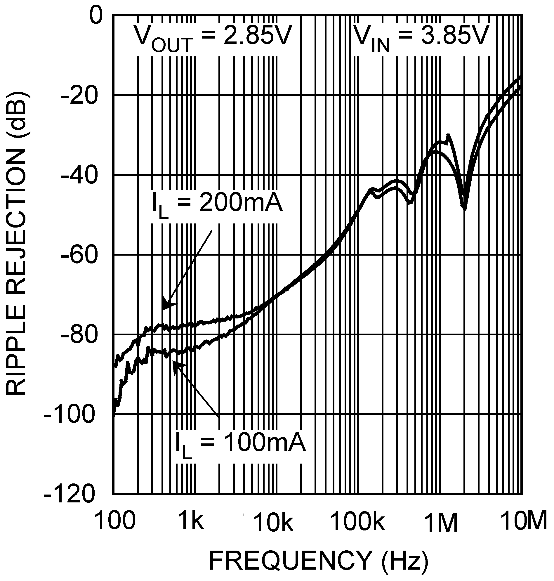 Figure 1. Power Supply Rejection Ratio
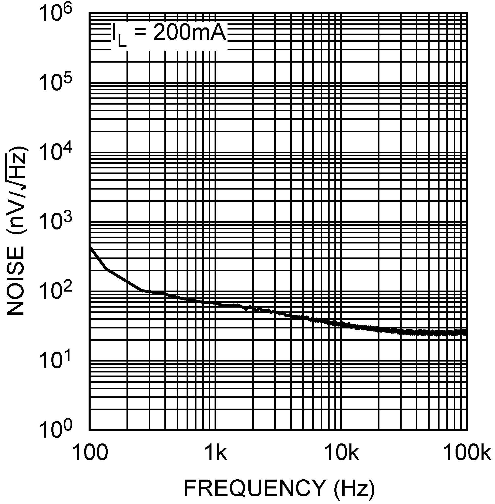 Figure 3. Noise Density
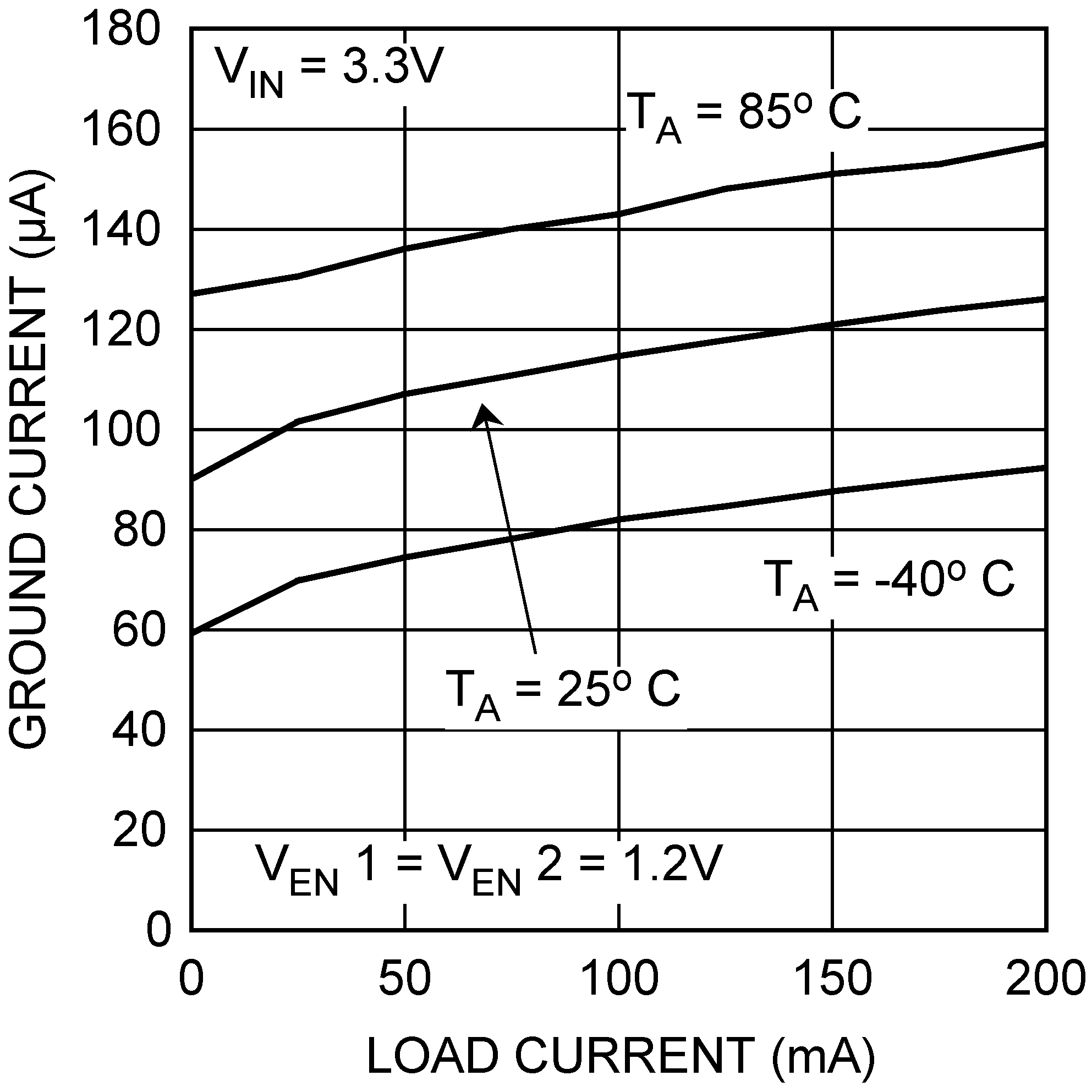 Figure 5. Ground Current vs Load Current
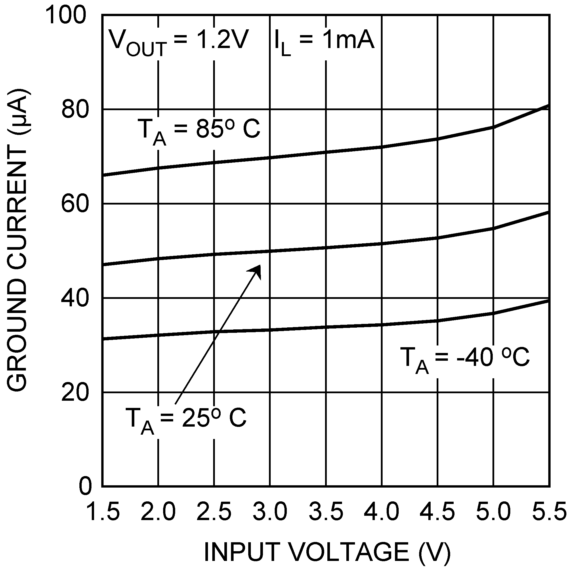 Figure 7. Ground Current vs VIN
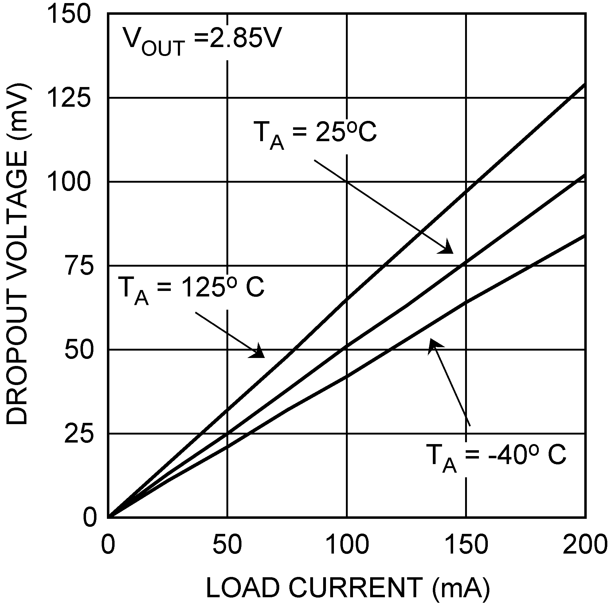 Figure 9. Dropout Voltage
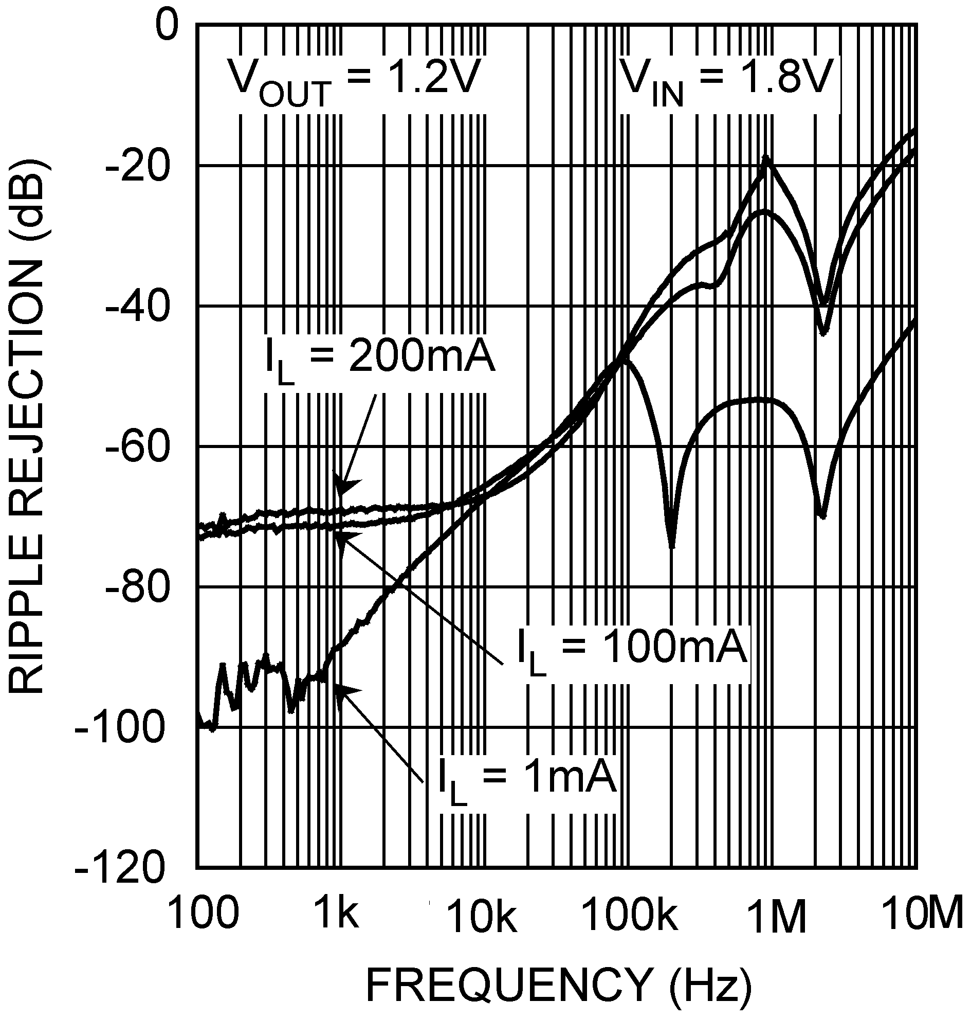 Figure 2. Power Supply Rejection Ratio
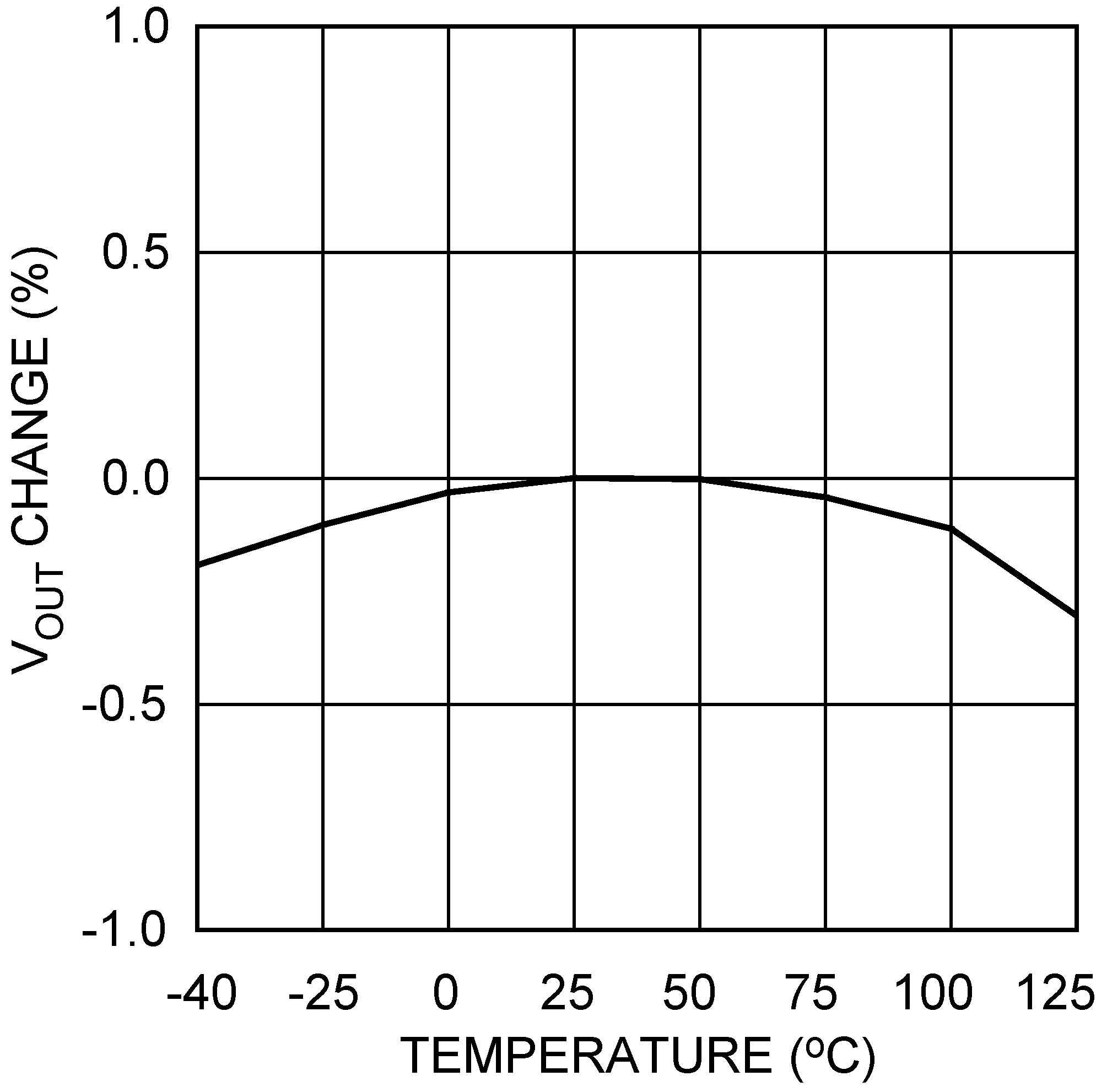 Figure 4. Output Voltage Change vs Temperature
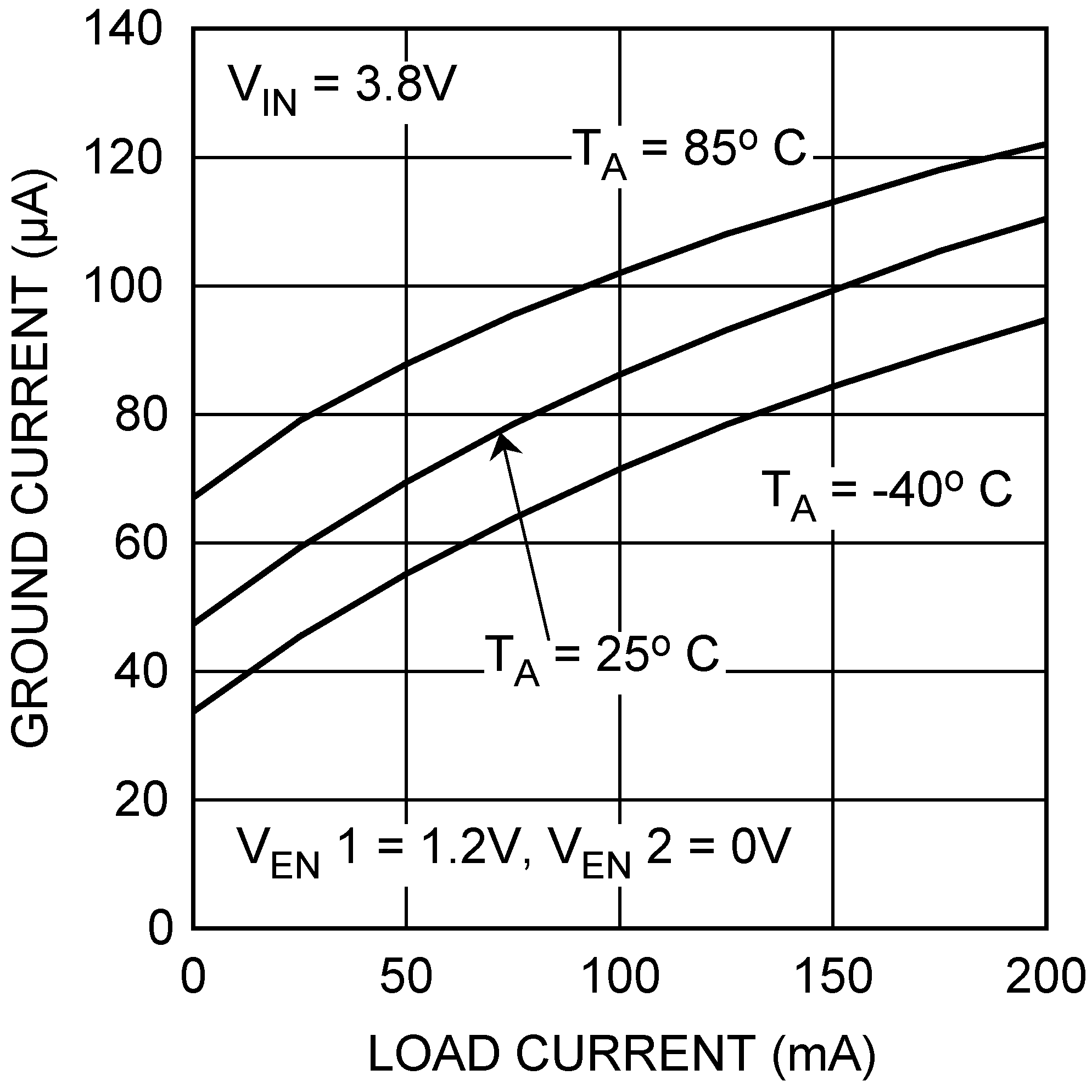 Figure 6. Ground Current vs Load Current
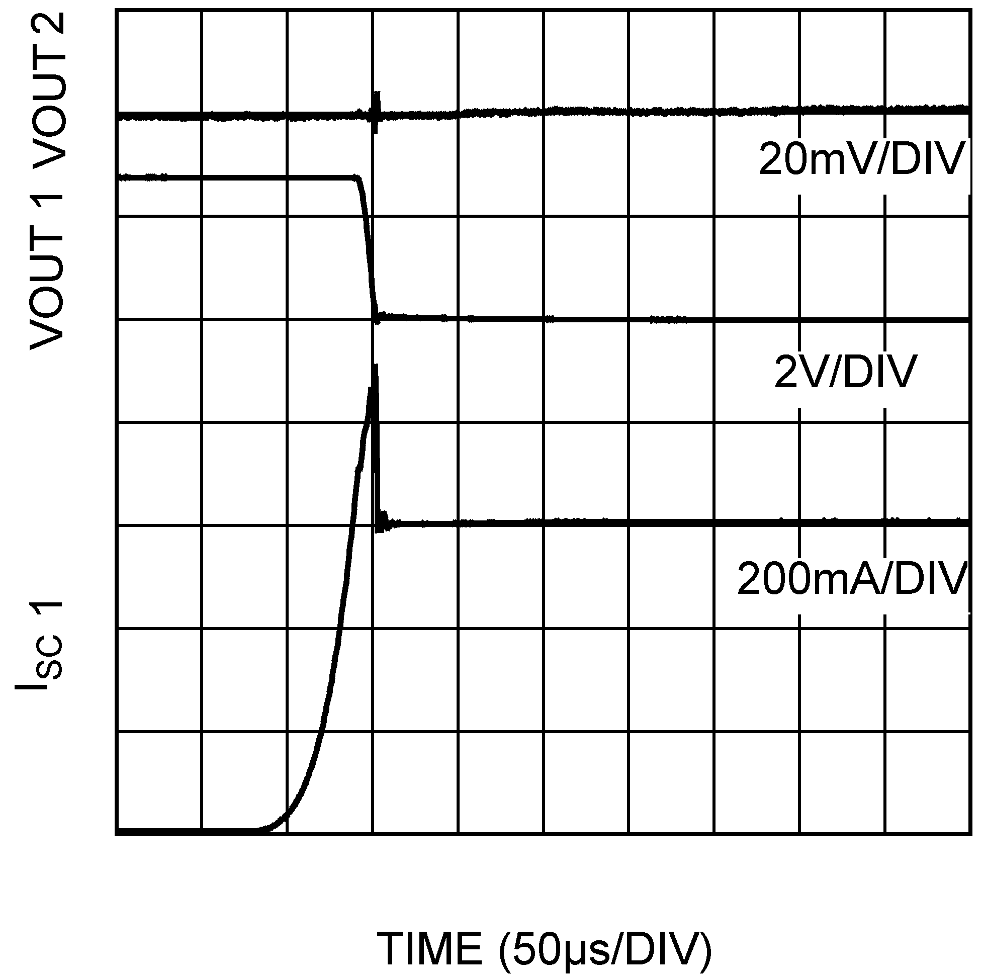 Figure 8. Short Circuit Current
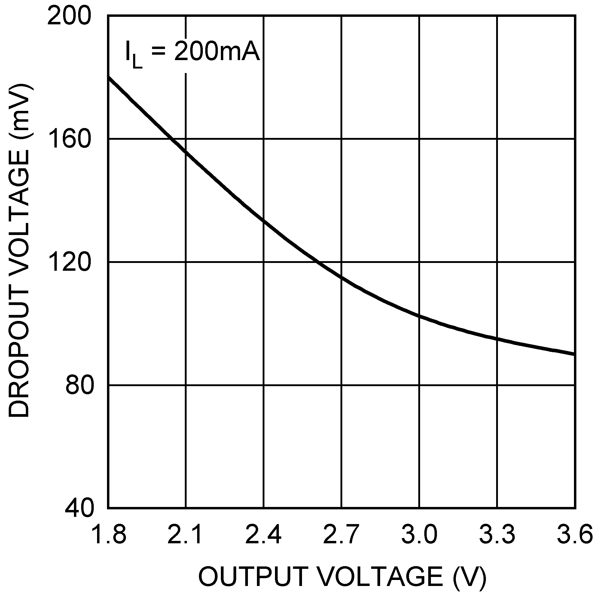 Figure 10. Dropout Voltage vs Output Voltage