SNOSB14E August 2009 – July 2024 LPV521
PRODUCTION DATA
- 1
- 1 Features
- 2 Applications
- 3 Description
- 4 Pin Configuration and Functions
- 5 Specifications
- 6 Detailed Description
- 7 Applications and Implementation
- 8 Device and Documentation Support
- 9 Revision History
- 10Mechanical, Packaging, and Orderable Information
Package Options
Refer to the PDF data sheet for device specific package drawings
Mechanical Data (Package|Pins)
- P|8
- DCK|5
Thermal pad, mechanical data (Package|Pins)
Orderable Information
3 Description
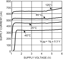
The LPV521 is a single, nanopower, 552nW amplifier designed for ultra-long-life battery applications. The operating voltage range of 1.6V to 5.5V coupled with typically 351nA of supply current make this device an excellent choice for RFID readers and remote-sensor nanopower applications. The device has an input common-mode voltage 0.1V over the rails, specified TCVOS, and voltage-swing-to-the-rail output performance. The LPV521 has a carefully designed CMOS input stage that outperforms competitors with typically 40fA IBIAS currents. This low input current significantly reduces IBIAS and IOS errors introduced in megohm resistance, high-impedance photodiode and charge sense applications. The LPV521 is a member of the PowerWise® family, and has an exceptional power-to-performance ratio.
The wide input common-mode voltage range, specified 1mV VOS and 3.5µV/°C TCVOS enables accurate and stable measurement for both high-side and low-side current sensing.
EMI protection is designed into the device to reduce sensitivity to unwanted RF signals from cell phones or other RFID readers.
The LPV521 is offered in 5-pin SC70 and 8-pin PDIP packages.
| PART NUMBER | PACKAGE(1) | PACKAGE SIZE(2) |
|---|---|---|
| LPV521 | DCK (SC70, 5) | 2mm × 2.1mm |
| P (PDIP, 8) | 9.81mm × 9.43mm |
 Nanopower Supply Current