SNOSAI6J September 2005 – August 2016 LPV7215
PRODUCTION DATA.
- 1 Features
- 2 Applications
- 3 Description
- 4 Revision History
- 5 Pin Configuration and Functions
- 6 Specifications
- 7 Detailed Description
- 8 Application and Implementation
- 9 Power Supply Recommendations
- 10Layout
- 11Device and Documentation Support
- 12Mechanical, Packaging, and Orderable Information
Package Options
Mechanical Data (Package|Pins)
Thermal pad, mechanical data (Package|Pins)
Orderable Information
6 Specifications
6.1 Absolute Maximum Ratings
over operating free-air temperature range (unless otherwise noted)(1)| MIN | MAX | UNIT | ||
|---|---|---|---|---|
| VIN differential | −2.5 | 2.5 | V | |
| Supply voltage (V+ - V−) | 6 | V | ||
| Voltage at input and output pins | V− − 0.3 | V+ + 0.3 | V | |
| Junction temperature, TJ (2) | 150 | °C | ||
| Storage temperature, Tstg | −65 | 150 | °C | |
(1) Stresses beyond those listed under Absolute Maximum Ratings may cause permanent damage to the device. These are stress ratings only, which do not imply functional operation of the device at these or any other conditions beyond those indicated under Recommended Operating Conditions. Exposure to absolute-maximum-rated conditions for extended periods may affect device reliability.
(2) The maximum power dissipation is a function of TJ(MAX), θJA. The maximum allowable power dissipation at any ambient temperature is PD = (TJ(MAX) – TA)/ θJA . All numbers apply for packages soldered directly onto a PCB.
6.2 ESD Ratings
| VALUE | UNIT | |||
|---|---|---|---|---|
| V(ESD) | Electrostatic discharge | Human-body model (HBM)(1) | ±2000 | V |
| Machine model (MM)(2) | ±200 | |||
(1) Human-body model, applicable std. MIL-STD-883, Method 3015.7.
(2) Machine model, applicable std. JESD22-A115-A (ESD MM std. of JEDEC)Field-Induced Charge-Device Model, applicable std. JESD22-C101-C (ESD FICDM std. of JEDEC).
6.3 Recommended Operating Conditions
over operating free-air temperature range (unless otherwise noted)| MIN | MAX | UNIT | ||
|---|---|---|---|---|
| Temperature(1) | –40 | 125 | °C | |
| Supply voltage (V+ – V−) | 1.8 | 5.5 | V | |
(1) The maximum power dissipation is a function of TJ(MAX), θJA. The maximum allowable power dissipation at any ambient temperature is PD = (TJ(MAX) – TA)/ θJA . All numbers apply for packages soldered directly onto a PCB.
6.4 Thermal Information
| THERMAL METRIC(1) | LPV7215 | UNIT | ||
|---|---|---|---|---|
| DBV (SOT-23) | DCK (SC70) | |||
| 5 PINS | 5 PINS | |||
| RθJA | Junction-to-ambient thermal resistance(2) | 234 | 456 | °C/W |
| RθJC(top) | Junction-to-case (top) thermal resistance | 153 | 110.8 | °C/W |
| RθJB | Junction-to-board thermal resistance | 51.7 | 59.8 | °C/W |
| ψJT | Junction-to-top characterization parameter | 38 | 3.6 | °C/W |
| ψJB | Junction-to-board characterization parameter | 51.2 | 59 | °C/W |
| RθJC(bot) | Junction-to-case (bottom) thermal resistance | n/a | n/a | °C/W |
(1) For more information about traditional and new thermal metrics, see the Semiconductor and IC Package Thermal Metrics application report.
(2) The maximum power dissipation is a function of TJ(MAX), θJA. The maximum allowable power dissipation at any ambient temperature is PD = (TJ(MAX) – TA)/ θJA . All numbers apply for packages soldered directly onto a PCB.
6.5 Electrical Characteristics: 1.8 V
Unless otherwise specified, all limits are specified for TA = 25°C, V+ = 1.8V, V− = 0 V, and VCM = V+/2, VO= V−.(1)| PARAMETER | TEST CONDITIONS | MIN (2) | TYP (3) | MAX (2) | UNIT | ||
|---|---|---|---|---|---|---|---|
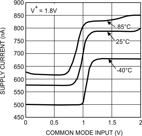
| IS | Supply current | VCM = 0.3 V | TA = 25°C | 580 | 750 | nA | |
| Temperature extremes | 1050 | ||||||
| VCM = 1.5 V | TA = 25°C | 790 | 980 | ||||
| Temperature extremes | 1300 | ||||||
| VOS | Input offset voltage | VCM = 0 V | TA = 25°C | ±0.3 | ±6 | mV | |
| Temperature extremes | ±8 | ||||||
| VCM = 1.8 V | TA = 25°C | ±0.4 | ±5 | ||||
| Temperature extremes | ±7 | ||||||
| TCVOS | Input offset average drift | See (4) | ±1 | µV/C | |||
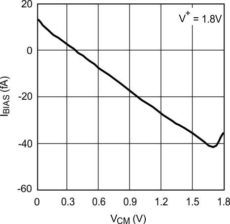
| IB | Input bias current (5) | VCM = 1.6 V | −40 | fA | |||
| IOS | Input offset current | 10 | fA | ||||
| CMRR | Common-mode rejection ratio | VCM Stepped from 0 V to 0.7 V | TA = 25°C | 66 | 88 | dB | |
| Temperature extremes | 62 | ||||||
| VCM Stepped from 1.2 V to 1.8 V | TA = 25°C | 68 | 87 | ||||
| Temperature extremes | 62 | ||||||
| VCM Stepped from 0 V to 1.8 V | TA = 25°C | 44 | 77 | ||||
| Temperature extremes | 43 | ||||||
| PSRR | Power supply rejection ratio | V+ = 1.8 V to 5.5 V, VCM = 0 V | TA = 25°C | 66 | 82 | dB | |
| Temperature extremes | 63 | ||||||
| CMVR | Input common-mode voltage range | CMRR ≥ 40 dB | Temperature Extremes | –0.1 | 1.9 | V | |
| AV | Voltage gain | 120 | dB | ||||
| VO | Output swing high | IO = 500 µA | TA = 25°C | 1.63 | 1.69 | V | |
| Temperature extremes | 1.58 | ||||||
| IO = 1 mA | TA = 25°C | 1.46 | 1.6 | ||||
| Temperature extremes | 1.37 | ||||||
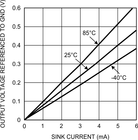
| Output swing low | IO = −500 µA | TA = 25°C | 88 | 180 | mV | ||
| Temperature extremes | 230 | ||||||
| IO = −1 mA | TA = 25°C | 180 | 310 | ||||
| Temperature extremes | 400 | ||||||
| IOUT | Output current | Source VO = V+/2 |
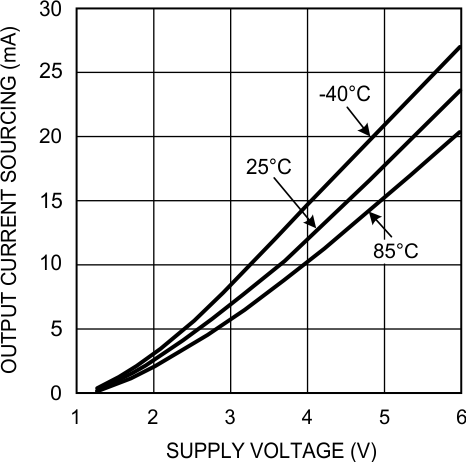
TA = 25°C | 1.75 | 2.26 | mA | |
| Temperature extremes | 1.3 | ||||||
| Sink VO = V+/2 |
TA = 25°C | 2.35 | 3.1 | ||||
| Temperature extremes | 1.45 | ||||||
| Propagation delay (high to low) |
Overdrive = 10 mV | 13 | µs | ||||
| Overdrive = 100 mV | TA = 25°C | 4.5 | 6.5 | ||||
| Temperature extremes | 9 | ||||||
| Propagation delay (low to high) |
Overdrive = 10 mV | 12.5 | µs | ||||
| Overdrive = 100 mV | TA = 25°C | 6.6 | 9 | ||||
| Temperature extremes | 12 | ||||||
| trise | Rise time | Overdrive = 10 mV CL = 30 pF, RL = 1 MΩ |
80 | ns | |||
| Overdrive = 100 mV CL = 30 pF, RL = 1 MΩ |
75 | ||||||
| tfall | Fall time | Overdrive = 10 mV CL = 30 pF, RL = 1 MΩ |
70 | ns | |||
| Overdrive = 100 mV CL = 30 pF, RL = 1 MΩ |
65 | ||||||
(1) Electrical table values apply only for factory testing conditions at the temperature indicated. Factory testing conditions result in very limited self-heating of the device.
(2) Limits are 100% production tested at 25°C. Limits over the operating temperature range are specified through correlations using statistical quality control (SQC) method.
(3) Typical values represent the most likely parametric norm as determined at the time of characterization. Actual typical values may vary over time and also depend on the application and configuration. The typical values are not tested and are not specified on shipped production material.
(4) Offset voltage average drift determined by dividing the change in VOS at temperature extremes into the total temperature change.
(5) Positive current corresponds to current flowing into the device.
6.6 Electrical Characteristics: 2.7 V
Unless otherwise specified, all limits are specified for TA = 25°C, V+ = 2.7 V, V− = 0 V, and VCM = V+/2, VO= V−.(1)| PARAMETER | TEST CONDITIONS | MIN (2) | TYP (3) | MAX (2) | UNIT | ||
|---|---|---|---|---|---|---|---|
| IS | Supply current | VCM = 0.3 V | TA = 25°C | 605 | 780 | nA | |
| Temperature extremes | 1100 | ||||||
| VCM = 2.4 V | TA = 25°C | 815 | 1010 | ||||
| Temperature extremes | 1350 | ||||||
| VOS | Input offset voltage | VCM = 0 V | TA = 25°C | ±0.3 | ±6 | mV | |
| Temperature extremes | ±8 | ||||||
| VCM = 2.7 V | TA = 25°C | ±0.3 | ±5 | ||||
| Temperature extremes | ±7 | ||||||
| TCVOS | Input offset average drift | See (4) | ±1 | µV/C | |||
| IB | Input bias current (5) | VCM = 1.8 V | −40 | fA | |||
| IOS | Input offset current | 20 | fA | ||||
| CMRR | Common-mode rejection ratio | VCM Stepped from 0 V to 1.6 V | TA = 25°C | 72 | 90 | dB | |
| Temperature extremes | 66 | ||||||
| VCM Stepped from 2.1V to 2.7V | TA = 25°C | 71 | 94 | ||||
| Temperature extremes | 63 | ||||||
| VCM Stepped from 0 V to 2.7 V | TA = 25°C | 47 | 80 | ||||
| Temperature extremes | 46 | ||||||
| PSRR | Power supply rejection ratio | V+ = 1.8 V to 5.5 V, VCM = 0 V | TA = 25°C | 66 | 82 | dB | |
| Temperature extremes | 63 | ||||||
| CMVR | Input common-mode voltage range | CMRR ≥ 40 dB | Temperature extremes | −0.1 | 2.8 | V | |
| AV | Voltage gain | 120 | dB | ||||
| VO | Output swing high | IO = 500 µA | TA = 25°C | 2.57 | 2.62 | V | |
| Temperature extremes | 2.53 | ||||||
| IO = 1 mA | TA = 25°C | 2.47 | 2.53 | ||||
| Temperature extremes | 2.4 | ||||||
| Output swing low | IO = −500 µA | TA = 25°C | 60 | 130 | mV | ||
| Temperature extremes | 190 | ||||||
| IO = −1 mA | TA = 25°C | 120 | 250 | ||||
| Temperature extremes | 330 | ||||||
| IOUT | Output current | Source VO = V+/2 |
TA = 25°C | 4.5 | 5.7 | mA | |
| Temperature extremes | 3.4 | ||||||
| Sink VO = V+/2 |
TA = 25°C | 5.6 | 7.5 | ||||
| Temperature extremes | 3.2 | ||||||
| Propagation delay (high to low) |
Overdrive = 10 mV | 14.5 | µs | ||||
| Overdrive = 100 mV | TA = 25°C | 5.8 | 8.5 | ||||
| Temperature extremes | 10.5 | ||||||
| Propagation delay (low to high) |
Overdrive = 10 mV | 15 | |||||
| Overdrive = 100 mV | TA = 25°C | 7.5 | 10 | ||||
| Temperature extremes | 12.5 | ||||||
| trise | Rise time | Overdrive = 10 mV CL = 30 pF, RL = 1 MΩ |
90 | ns | |||
| Overdrive = 100 mV CL = 30 pF, RL = 1 MΩ |
85 | ||||||
| tfall | Fall time | Overdrive = 10 mV CL = 30 pF, RL = 1 MΩ |
85 | ns | |||
| Overdrive = 100 mV CL = 30 pF, RL = 1 MΩ |
75 | ||||||
(1) Electrical table values apply only for factory testing conditions at the temperature indicated. Factory testing conditions result in very limited self-heating of the device.
(2) Limits are 100% production tested at 25°C. Limits over the operating temperature range are specified through correlations using statistical quality control (SQC) method.
(3) Typical values represent the most likely parametric norm as determined at the time of characterization. Actual typical values may vary over time and also depend on the application and configuration. The typical values are not tested and are not specified on shipped production material.
(4) Offset voltage average drift determined by dividing the change in VOS at temperature extremes into the total temperature change.
(5) Positive current corresponds to current flowing into the device.
6.7 Electrical Characteristics: 5 V
Unless otherwise specified, all limits are specified for TA = 25°C, V+ = 5 V, V− = 0 V, and VCM = V+/2, VO= V−. (1)| PARAMETER | TEST CONDITIONS | MIN (2)
|
TYP (3)
|
MAX (2)
|
UNIT | ||
|---|---|---|---|---|---|---|---|
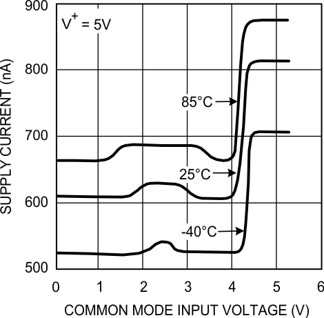
| IS | Supply current | VCM = 0.3 V | TA = 25°C | 612 | 790 | nA | |
| Temperature extremes | 1150 | ||||||
| VCM = 4.7 V | TA = 25°C | 825 | 1030 | ||||
| Temperature extremes | 1400 | ||||||
| VOS | Input offset voltage | VCM = 0 V | TA = 25°C | ±0.3 | ±6 | mV | |
| Temperature extremes | ±8 | ||||||
| VCM = 5 V | TA = 25°C | ±5 | |||||
| Temperature extremes | ±7 | ||||||
| TCVOS | Input offset average drift | See (4) | ±1 | µV/C | |||
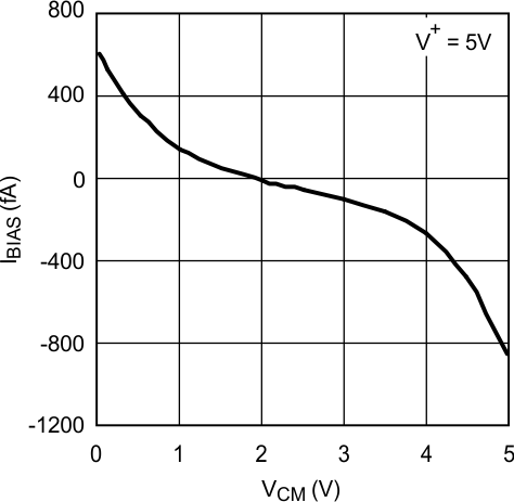
| IB | Input bias current (5) | VCM = 4.5 V | −400 | fA | |||
| IOS | Input offset current | 20 | fA | ||||
| CMRR | Common-mode rejection ratio | VCM Stepped from 0 V to 3.9 V | TA = 25°C | 72 | 98 | dB | |
| Temperature extremes | 66 | ||||||
| VCM Stepped from 4.4 V to 5 V | TA = 25°C | 73 | 92 | ||||
| Temperature extremes | 67 | ||||||
| VCM Stepped from 0 V to 5 V | TA = 25°C | 53 | 82 | ||||
| Temperature extremes | 49 | ||||||
| PSRR | Power supply rejection ratio | V+ = 1.8 V to 5.5 V, VCM = 0 V | TA = 25°C | 66 | 82 | dB | |
| Temperature extremes | 63 | ||||||
| CMVR | Input common-mode voltage range | CMRR ≥ 40 dB | Temperature extremes | −0.1 | 5.1 | V | |
| AV | Voltage gain | 120 | dB | ||||
| VO | Output swing high | IO = 500 µA | TA = 25°C | 4.9 | 4.94 | V | |
| Temperature extremes | 4.86 | ||||||
| IO = 1 mA | TA = 25°C | 4.82 | 4.89 | ||||
| Temperature extremes | 4.77 | ||||||
| Output swing low | IO = −500 µA | TA = 25°C | 43 | 90 | mV | ||
| Temperature extremes | 130 | ||||||
| IO = −1 mA | TA = 25°C | 88 | 170 | ||||
| Temperature extremes | 230 | ||||||
| IOUT | Output current | Source VO = V+/2 |
TA = 25°C | 13 | 17 | mA | |
| Temperature extremes | 7.5 | ||||||
| Sink VO = V+/2 |
TA = 25°C | 14.5 | 19 | ||||
| Temperature extremes | 8.5 | ||||||
| Propagation delay (high to low) |
Overdrive = 10 mV | 18 | µs | ||||
| Overdrive = 100 mV | TA = 25°C | 7.7 | 13.5 | ||||
| Temperature extremes | 16 | ||||||
| Propagation delay (low to high) |
Overdrive = 10 mV | 30 | µs | ||||
| Overdrive = 100 mV | TA = 25°C | 12 | 15 | ||||
| Temperature extremes | 20 | ||||||
| trise | Rise time | Overdrive = 10 mV CL = 30 pF, RL = 1 MΩ |
100 | ns | |||
| Overdrive = 100 mV CL = 30 pF, RL = 1 MΩ |
100 | ||||||
| tfall | Fall time | Overdrive = 10 mV CL = 30 pF, RL = 1 MΩ |
115 | ns | |||
| Overdrive = 100 mV CL = 30 pF, RL = 1 MΩ |
95 | ||||||
(1) Electrical table values apply only for factory testing conditions at the temperature indicated. Factory testing conditions result in very limited self-heating of the device.
(2) Limits are 100% production tested at 25°C. Limits over the operating temperature range are specified through correlations using statistical quality control (SQC) method.
(3) Typical values represent the most likely parametric norm as determined at the time of characterization. Actual typical values may vary over time and also depend on the application and configuration. The typical values are not tested and are not specified on shipped production material.
(4) Offset voltage average drift determined by dividing the change in VOS at temperature extremes into the total temperature change.
(5) Positive current corresponds to current flowing into the device.
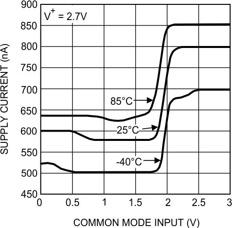
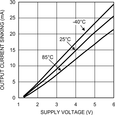
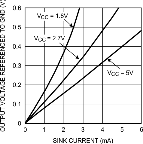
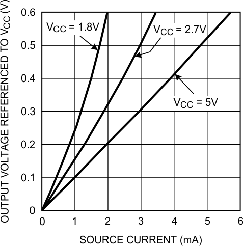
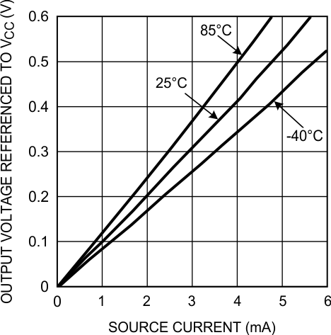
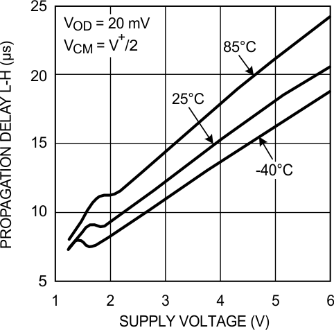
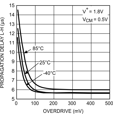
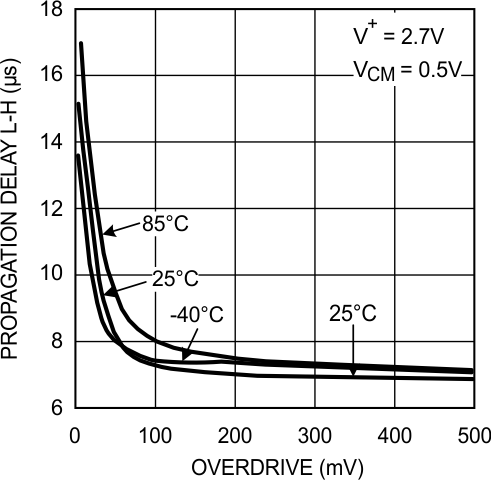
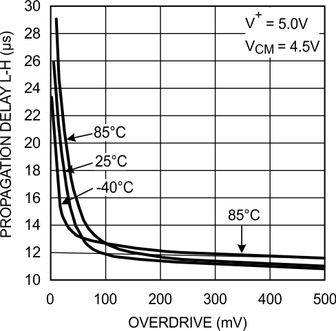
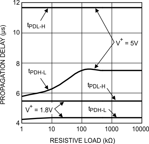
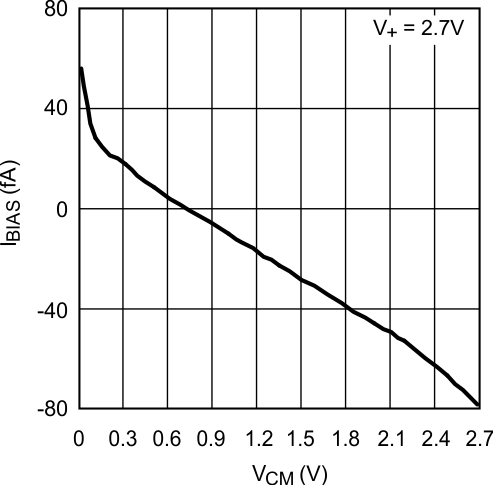
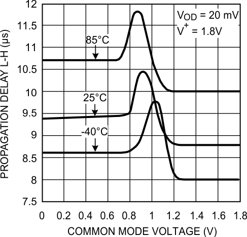
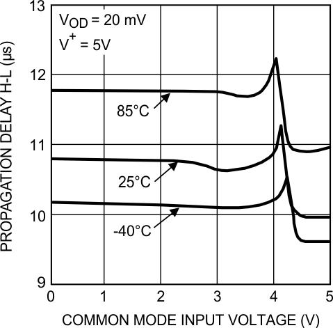
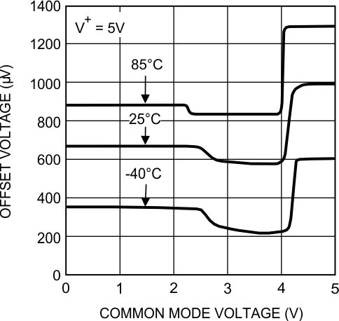
6.8 Typical Characteristics
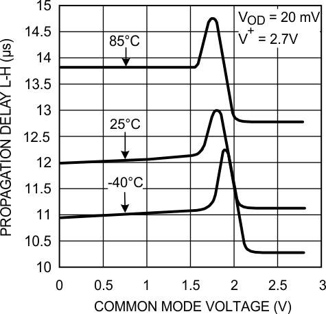
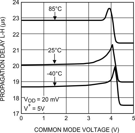
At TJ = 25°C unless otherwise specified.
