SDLS973 june 2023 LSF0101
PRODUCTION DATA
- 1
- 1 Features
- 2 Applications
- 3 Description
- 4 Revision History
- 5 Pin Configuration and Functions
-
6 Specifications
- 6.1 Absolute Maximum Ratings
- 6.2 ESD Ratings
- 6.3 Recommended Operating Conditions
- 6.4 Thermal Information
- 6.5 Electrical Characteristics
- 6.6 LSF0101 AC Performance (Translating Down) Switching Characteristics , VCCB = 3.3 V
- 6.7 LSF0101 AC Performance (Translating Down) Switching Characteristics, VCCB = 2.5 V
- 6.8 LSF0101 AC Performance (Translating Up) Switching Characteristics, VCCB = 3.3 V
- 6.9 LSF0101 AC Performance (Translating Up) Switching Characteristics, VCCB = 2.5 V
- 6.10 Typical Characteristics
- 7 Parameter Measurement Information
- 8 Detailed Description
- 9 Application and Implementation
- 10Power Supply Recommendations
- 11Layout
- 12Device and Documentation Support
- 13Mechanical, Packaging, and Orderable Information
Package Options
Mechanical Data (Package|Pins)
Thermal pad, mechanical data (Package|Pins)
- DRY|6
Orderable Information
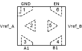
5 Pin Configuration and Functions
Pinout drawings are not to scale
Pinout drawings are not to scale Figure 5-1 LSF0101 DRY Package,
6-Pin SON
(Transparent Top View). Pinout drawings are not to scale
 Figure 5-1 LSF0101 DRY Package,
6-Pin SON
(Transparent Top View). Pinout drawings are not to scale
Figure 5-1 LSF0101 DRY Package,
6-Pin SON
(Transparent Top View). Pinout drawings are not to scalePinout drawings are not to scale Figure 5-2 LSF0101 DTQ Package,
6-Pin X2SON
(Transparent Top View). Pinout drawings are not to scale
 Figure 5-2 LSF0101 DTQ Package,
6-Pin X2SON
(Transparent Top View). Pinout drawings are not to scale
Figure 5-2 LSF0101 DTQ Package,
6-Pin X2SON
(Transparent Top View). Pinout drawings are not to scaleTable 5-1 Pin Functions
| PIN | TYPE(1) | DESCRIPTION | |
|---|---|---|---|
| NAME | NO. | ||
| A1 | 3 | I/O | Input/Output A port for Channel 1 |
| B1 | 4 | I/O | Input/Output B port for Channel 1 |
| EN | 6 | I | I/O enable input; see Section 9.2.1.2.1 for typical setup. Should be tied directly to Vref_B to be enabled or pulled LOW to disable all I/O pins. |
| GND | 1 | — | Ground |
| Vref_A | 2 | — | A side reference supply voltage; see Section 9 for setup and supply voltage range. |
| Vref_B | 5 | — | B side reference supply voltage. Must be connected to supply through 200 kΩ; see Section 9 for setup and supply voltage range. |
(1) I = input, O = output