SLVSCP5H July   2014  – April 2021 LSF0204 , LSF0204D

PRODUCTION DATA  

  1. Features
  2. Applications
  3. Description
  4. Revision History
  5. Description (continued)
  6. Pin Configuration and Functions
  7. Specifications
    1. 7.1  Absolute Maximum Ratings
    2. 7.2  ESD Ratings
    3. 7.3  Recommended Operating Conditions
    4. 7.4  Thermal Information
    5. 7.5  Electrical Characteristics
    6. 7.6  Switching Characteristics: AC Performance (Translating Down, 3.3 V to 1.8 V)
    7. 7.7  Switching Characteristics: AC Performance (Translating Down, 3.3 V to 1.2 V)
    8. 7.8  Switching Characteristics: AC Performance (Translating Up, 1.8 V to 3.3 V)
    9. 7.9  Switching Characteristics: AC Performance (Translating Up, 1.2 V to 1.8 V)
    10. 7.10 Typical Characteristics
  8. Parameter Measurement Information
    1. 8.1 Load Circuit AC Waveform for Outputs
  9. Detailed Description
    1. 9.1 Overview
    2. 9.2 Functional Block Diagram
    3. 9.3 Feature Description
      1. 9.3.1 Support High Speed Translation, Greater than 100 MHz
      2. 9.3.2 Bidirectional Voltage Translation Without DIR Terminal
      3. 9.3.3 5-V Tolerance on IO Port and 125°C Support
      4. 9.3.4 Channel Specific Translation
      5. 9.3.5 Ioff, Partial Power Down Mode
    4. 9.4 Device Functional Modes
  10. 10Application and Implementation
    1. 10.1 Application Information
    2. 10.2 Typical Applications
      1. 10.2.1 I2C PMBus, SMBus, GPIO, Application
        1. 10.2.1.1 Design Requirements
          1. 10.2.1.1.1 Enable, Disable, and Reference Voltage Guidelines
        2. 10.2.1.2 Detailed Design Procedure
          1. 10.2.1.2.1 Bidirectional Translation
            1. 10.2.1.2.1.1 Pull-Up Resistor Sizing
          2. 10.2.1.2.2 LS Family Bandwidth
        3. 10.2.1.3 Application Curve
      2. 10.2.2 MDIO Application
        1. 10.2.2.1 Design Requirements
        2. 10.2.2.2 Detailed Design Procedure
        3. 10.2.2.3 Application Curve
      3. 10.2.3 Multiple Voltage Translation in Single Device, Application
        1. 10.2.3.1 Design Requirements
        2. 10.2.3.2 Detailed Design Procedure
        3. 10.2.3.3 Application Curve
  11. 11Power Supply Recommendations
  12. 12Layout
    1. 12.1 Layout Guidelines
    2. 12.2 Layout Example
  13. 13Device and Documentation Support
    1. 13.1 Receiving Notification of Documentation Updates
    2. 13.2 Support Resources
    3. 13.3 Trademarks
    4. 13.4 Electrostatic Discharge Caution
    5. 13.5 Glossary
  14. 14Mechanical, Packaging, and Orderable Information

Package Options

Refer to the PDF data sheet for device specific package drawings

Mechanical Data (Package|Pins)
  • RGY|14
  • YZP|12
  • RUT|12
  • PW|14
Thermal pad, mechanical data (Package|Pins)
Orderable Information

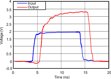
Typical Characteristics

GUID-A9752A4E-7F40-47D6-B14F-0DD910DDA4AF-low.gifFigure 7-1 Signal Integrity (1.8 V to 3.3 V Translation Up at 50 MHz)