SLOS018I May 1988 – July 2016 LT1013 , LT1013AM , LT1013D , LT1013M
PRODUCTION DATA.
- 1 Features
- 2 Applications
- 3 Description
- 4 Revision History
- 5 Pin Configuration and Functions
-
6 Specifications
- 6.1 Absolute Maximum Ratings
- 6.2 ESD Ratings
- 6.3 Recommended Operating Conditions
- 6.4 Thermal Information
- 6.5 Electrical Characteristics: LT1013C, ±15 V
- 6.6 Electrical Characteristics: LT1013C, 5 V
- 6.7 Electrical Characteristics: LT1013D, ±15 V
- 6.8 Electrical Characteristics: LT1013D, 5 V
- 6.9 Electrical Characteristics: LT1013DI, ±15 V
- 6.10 Electrical Characteristics: LT1013DI, 5 V
- 6.11 Electrical Characteristics: LT1013M, ±15 V
- 6.12 Electrical Characteristics: LT1013M, 5 V
- 6.13 Electrical Characteristics: LT1013AM, ±15 V
- 6.14 Electrical Characteristics: LT1013AM, 5 V
- 6.15 Electrical Characteristics: LT1013DM, ±15 V
- 6.16 Electrical Characteristics: LT1013DM, 5 V
- 6.17 Operating Characteristics
- 6.18 Typical Characteristics
- 7 Detailed Description
- 8 Application and Implementation
- 9 Power Supply Recommendations
- 10Layout
- 11Device and Documentation Support
- 12Mechanical, Packaging, and Orderable Information
Package Options
Mechanical Data (Package|Pins)
Thermal pad, mechanical data (Package|Pins)
Orderable Information
8 Application and Implementation
NOTE
Information in the following applications sections is not part of the TI component specification, and TI does not warrant its accuracy or completeness. TI’s customers are responsible for determining suitability of components for their purposes. Customers should validate and test their design implementation to confirm system functionality.
8.1 Application Information
The LT1013x operational amplifiers are useful in a wide range of signal conditioning applications where high DC accuracy is needed.
8.2 Typical Application
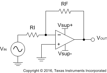
A typical application for an operational amplifier in an inverting amplifier. This amplifier takes a positive voltage on the input and makes it a negative voltage of the same magnitude. In the same manner, it also makes negative voltages positive.
 Figure 27. Application Schematic
8.2.1 Design Requirements
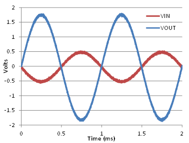
The supply voltage must be chosen such that it is larger than the input voltage range and output range. For instance, this application scales a signal of ±0.5 V to ±1.8 V. Setting the supply at ±12 V is sufficient to accommodate this application.
8.2.2 Detailed Design Procedure
Determine the gain required by the inverting amplifier using Equation 1 and Equation 2:


Once the desired gain is determined, choose a value for RI or RF. Choosing a value in the kΩ range is desirable because the amplifier circuit will use currents in the milliamp range. This ensures the part does not draw too much current. This example chooses 10 kΩ for RI, which means 36 kΩ is used for RF. This was determined by Equation 3.

8.2.3 Application Curve
 Figure 28. Input and Output Voltages of the Inverting Amplifier