SLOS018I May 1988 – July 2016 LT1013 , LT1013AM , LT1013D , LT1013M
PRODUCTION DATA.
- 1 Features
- 2 Applications
- 3 Description
- 4 Revision History
- 5 Pin Configuration and Functions
-
6 Specifications
- 6.1 Absolute Maximum Ratings
- 6.2 ESD Ratings
- 6.3 Recommended Operating Conditions
- 6.4 Thermal Information
- 6.5 Electrical Characteristics: LT1013C, ±15 V
- 6.6 Electrical Characteristics: LT1013C, 5 V
- 6.7 Electrical Characteristics: LT1013D, ±15 V
- 6.8 Electrical Characteristics: LT1013D, 5 V
- 6.9 Electrical Characteristics: LT1013DI, ±15 V
- 6.10 Electrical Characteristics: LT1013DI, 5 V
- 6.11 Electrical Characteristics: LT1013M, ±15 V
- 6.12 Electrical Characteristics: LT1013M, 5 V
- 6.13 Electrical Characteristics: LT1013AM, ±15 V
- 6.14 Electrical Characteristics: LT1013AM, 5 V
- 6.15 Electrical Characteristics: LT1013DM, ±15 V
- 6.16 Electrical Characteristics: LT1013DM, 5 V
- 6.17 Operating Characteristics
- 6.18 Typical Characteristics
- 7 Detailed Description
- 8 Application and Implementation
- 9 Power Supply Recommendations
- 10Layout
- 11Device and Documentation Support
- 12Mechanical, Packaging, and Orderable Information
Package Options
Mechanical Data (Package|Pins)
Thermal pad, mechanical data (Package|Pins)
Orderable Information
6 Specifications
6.1 Absolute Maximum Ratings
over operating free-air temperature range (unless otherwise noted)(1)| MIN | MAX | UNIT | |||
|---|---|---|---|---|---|
| VCC+ – VCC– | Supply voltage(2) | –0.3 | 44 | V | |
| VI | Input voltage (any input) | VCC– – 5 | VCC+ | V | |
| Differential input voltage(3) | ±30 | V | |||
| Duration of short-circuit current at (or below) 25°C(4) | Unlimited | ||||
| Case temperature for 60 s | FK package | 260 | °C | ||
| Lead temperature 1,6 mm (1/16 inch) from case for 10 s |
JG package | 300 | °C | ||
| TJ | Operating virtual junction temperature | 150 | °C | ||
| Tstg | Storage temperature | –65 | 150 | °C | |
(1) Stresses beyond those listed under Absolute Maximum Ratings may cause permanent damage to the device. These are stress ratings only, which do not imply functional operation of the device at these or any other conditions beyond those indicated under Recommended Operating Conditions. Exposure to absolute-maximum-rated conditions for extended periods may affect device reliability.
(2) Supply voltage is VCC+ with respect to VCC–.
(3) Differential voltage is IN+ with respect to IN−.
(4) The output may be shorted to either supply.
6.2 ESD Ratings
| VALUE | UNIT | |||
|---|---|---|---|---|
| LT1013 in D and P packages | ||||
| V(ESD) | Electrostatic discharge | Human-body model (HBM), per ANSI/ESDA/JEDEC JS-001(1) | ±1000 | V |
| Charged-device model (CDM), per JEDEC specification JESD22-C101(2) | ±500 | |||
| LT1013D in D and P packages | ||||
| V(ESD) | Electrostatic discharge | Human-body model (HBM), per ANSI/ESDA/JEDEC JS-001(1) | ±1000 | V |
| Charged-device model (CDM), per JEDEC specification JESD22-C101(2) | ±500 | |||
(1) JEDEC document JEP155 states that 500-V HBM allows safe manufacturing with a standard ESD control process.
(2) JEDEC document JEP157 states that 250-V CDM allows safe manufacturing with a standard ESD control process.
6.3 Recommended Operating Conditions
over operating free-air temperature range (unless otherwise noted)| MIN | MAX | UNIT | |||
|---|---|---|---|---|---|
| VCC+ – VCC– | Supply voltage | 5 | 30 | V | |
| TA | Ambient temperature | LT1013C, LT1013D | 0 | 70 | °C |
| LT1013DI | –40 | 105 | |||
| LT1013M, LT1013AM, LT1013DM | –55 | 125 | |||
| VICM | Input common-mode voltage | LT1013C, LT1013D, LT1013DI | VCC– | VCC+ – 2 | V |
| LT1013M, LT1013AM, LT1013DM | VCC- + 0.1 | VCC+ – 2 | |||
6.4 Thermal Information
| THERMAL METRIC(1) | LT1013x | UNIT | ||||
|---|---|---|---|---|---|---|
| D (SOIC) | P (PDIP) | FK (LCCC) | JG (CDIP) | |||
| 8 PINS | 8 PINS | 20 PINS | 8 PINS | |||
| RθJA | Junction-to-ambient thermal resistance(2)(3) | 101.6 | 49.5 | — | — | °C/W |
| RθJC(top) | Junction-to-case (top) thermal resistance | 47.6 | 38.7 | 35.7(4) | 58.5(4) | °C/W |
| RθJB | Junction-to-board thermal resistance | 42 | 26.7 | 34.8 | 82.9 | °C/W |
| ψJT | Junction-to-top characterization parameter | 8.3 | 15.9 | — | — | °C/W |
| ψJB | Junction-to-board characterization parameter | 41.5 | 26.6 | — | — | °C/W |
| RθJC(bot) | Junction-to-case (bottom) thermal resistance | — | — | 4.0(4) | 10.8(4) | °C/W |
(1) For more information about traditional and new thermal metrics, see the Semiconductor and IC Package Thermal Metrics application report.
(2) Maximum power dissipation is a function of TJ(max), RθJA, and TA. The maximum allowable power dissipation at any allowable ambient temperature is PD = (TJ(max) − TA )/ RθJA. Operating at the absolute maximum TJ of 150°C can affect reliability. Due to variation in individual device electrical characteristics and thermal resistance, the built-in thermal overload protection may be activated at power levels slightly above or below the rated dissipation.
(3) The package thermal impedance is calculated in accordance with JESD 51-7.
(4) RθJC(top) and RθJC(bot)thermal impedances are calculated in accordance with MIL-STD-883 for LCCC and CDIP
6.5 Electrical Characteristics: LT1013C, ±15 V
at specified free-air temperature, VCC± = ±15 V, VIC = 0 (unless otherwise noted)| PARAMETER | TEST CONDITIONS | TA(1) | MIN | TYP(2) | MAX | UNIT | |
|---|---|---|---|---|---|---|---|
| VIO | Input offset voltage | RS = 50 Ω | 25°C | 60 | 300 | µV | |
| Full range | 400 | ||||||
| αVIO | Temperature coefficient of input offset voltage | Full range | 0.4 | 2.5 | µV/°C | ||
| Long-term drift of input offset voltage | 25°C | 0.5 | µV/mo | ||||
| IIO | Input offset current | 25°C | 0.2 | 1.5 | nA | ||
| Full range | 2.8 | ||||||
| IIB | Input bias current | 25°C | –15 | –30 | nA | ||
| Full range | –38 | ||||||
| VICR | Common-mode input voltage range | Recommended range | 25°C | –15 | 13.5 | V | |
| Full range | –15 | 13 | |||||
| VOM | Maximum peak output voltage swing | RL = 2 kΩ | 25°C | ±12.5 | ±14 | V | |
| Full range | ±12 | ||||||
| AVD | Large-signal differential voltage amplification | VO = ±10 V, RL = 600 Ω | 25°C | 0.5 | 0.2 | V/µV | |
| VO = ±10 V, RL = 2 kΩ | 25°C | 1.2 | 7 | ||||
| Full range | 0.7 | ||||||
| CMRR | Common-mode rejection ratio | VIC = −15 V to 13.5 V | 25°C | 97 | 114 | dB | |
| VIC = −14.9 V to 13 V | Full range | 94 | |||||
| kSVR | Supply-voltage rejection ratio (ΔVCC/ΔVIO) | VCC+ = ±2 V to ±18 V | 25°C | 100 | 117 | dB | |
| Full range | 97 | ||||||
| Channel separation | VO = ±10 V, RL = 2 kΩ | 25°C | 120 | 137 | dB | ||
| rid | Differential input resistance | 25°C | 70 | 300 | MΩ | ||
| ric | Common-mode input resistance | 25°C | 4 | GΩ | |||
| ICC | Supply current per amplifier | 25°C | 0.35 | 0.55 | mA | ||
| Full range | 0.7 | ||||||
(1) Full range is 0°C to 70°C.
(2) All typical values are at TA = 25°C.
6.6 Electrical Characteristics: LT1013C, 5 V
at specified free-air temperature, VCC+ = 5 V, VCC– = 0, VO = 1.4 V, VIC = 0 (unless otherwise noted)| PARAMETER | TEST CONDITIONS | TA(1) | MIN | TYP(2) | MAX | UNIT | |
|---|---|---|---|---|---|---|---|
| VIO | Input offset voltage | RS = 50 Ω | 25°C | 90 | 450 | µV | |
| Full range | 570 | ||||||
| IIO | Input offset current | 25°C | 0.3 | 2 | nA | ||
| Full range | 6 | ||||||
| IIB | Input bias current | 25°C | –18 | –50 | nA | ||
| Full range | –90 | ||||||
| VICR | Common-mode input voltage range | Recommended range | 25°C | 0 | 3.5 | V | |
| Full range | 0 | 3 | |||||
| VOM | Maximum peak output voltage swing | Output low, No load | 25°C | 15 | 25 | V | |
| Output low, RL = 600 Ω to GND | 25°C | 5 | 10 | ||||
| Full range | 13 | ||||||
| Output low, Isink = 1 mA | 25°C | 220 | 350 | ||||
| Output high, No load | 25°C | 4 | 4.4 | ||||
| Output high, RL = 600 Ω to GND | 25°C | 3.4 | 4 | ||||
| Full range | 3.2 | ||||||
| AVD | Large-signal differential voltage amplification | VO = 5 mV to 4 V, RL = 500 Ω | 25°C | 1 | V/µV | ||
| ICC | Supply current per amplifier | 25°C | 0.32 | 0.5 | mA | ||
| Full range | 0.55 | ||||||
(1) Full range is 0°C to 70°C.
(2) All typical values are at TA = 25°C.
6.7 Electrical Characteristics: LT1013D, ±15 V
at specified free-air temperature, VCC± = ±15 V, VIC = 0 (unless otherwise noted)| PARAMETER | TEST CONDITIONS | TA(1) | MIN | TYP(2) | MAX | UNIT | |
|---|---|---|---|---|---|---|---|
| VIO | Input offset voltage | RS = 50 Ω | 25°C | 200 | 800 | µV | |
| Full range | 1000 | ||||||
| αVIO | Temperature coefficient of input offset voltage | Full range | 0.7 | 5 | µV/°C | ||
| Long-term drift of input offset voltage | 25°C | 0.5 | µV/mo | ||||
| IIO | Input offset current | 25°C | 0.2 | 1.5 | nA | ||
| Full range | 2.8 | ||||||
| IIB | Input bias current | 25°C | –15 | –30 | nA | ||
| Full range | –38 | ||||||
| VICR | Common-mode input voltage range | Recommended range | 25°C | –15 | 13.5 | V | |
| Full range | –15 | 13 | |||||
| VOM | Maximum peak output voltage swing | RL = 2 kΩ | 25°C | ±12.5 | ±14 | V | |
| Full range | ±12 | ||||||
| AVD | Large-signal differential voltage amplification | VO = ±10 V, RL = 600 Ω | 25°C | 0.5 | 2 | V/µV | |
| VO = ±10 V, RL = 2 kΩ | 25°C | 1.2 | 7 | ||||
| Full range | 0.7 | ||||||
| CMRR | Common-mode rejection ratio | VIC = −15 V to 13.5 V | 25°C | 97 | 114 | dB | |
| VIC = −14.9 V to 13 V | Full range | 94 | |||||
| kSVR | Supply-voltage rejection ratio (ΔVCC/ΔVIO) | VCC+ = ±2 V to ±18 V | 25°C | 100 | 117 | dB | |
| Full range | 97 | ||||||
| Channel separation | VO = ±10 V, RL = 2 kΩ | 25°C | 120 | 137 | dB | ||
| rid | Differential input resistance | 25°C | 70 | 300 | MΩ | ||
| ric | Common-mode input resistance | 25°C | 4 | GΩ | |||
| ICC | Supply current per amplifier | 25°C | 0.35 | 0.55 | mA | ||
| Full range | 0.6 | ||||||
(1) Full range is 0°C to 70°C.
(2) All typical values are at TA = 25°C.
6.8 Electrical Characteristics: LT1013D, 5 V
at specified free-air temperature, VCC+ = 5 V, VCC– = 0, VO = 1.4 V, VIC = 0 (unless otherwise noted)| PARAMETER | TEST CONDITIONS | TA(1) | MIN | TYP(2) | MAX | UNIT | |
|---|---|---|---|---|---|---|---|
| VIO | Input offset voltage | RS = 50 Ω | 25°C | 250 | 950 | µV | |
| Full range | 1200 | ||||||
| IIO | Input offset current | 25°C | 0.3 | 2 | nA | ||
| Full range | 6 | ||||||
| IIB | Input bias current | 25°C | –18 | –50 | nA | ||
| Full range | –90 | ||||||
| VICR | Common-mode input voltage range | Recommended range | 25°C | 0 | 3.5 | V | |
| Full range | 0 | 3 | |||||
| VOM | Maximum peak output voltage swing | Output low, No load | 25°C | 15 | 25 | V | |
| Output low, RL = 600 Ω to GND | 25°C | 5 | 10 | ||||
| Full range | 13 | ||||||
| Output low, Isink = 1 mA | 25°C | 220 | 350 | ||||
| Output high, No load | 25°C | 4 | 4.4 | ||||
| Output high, RL = 600 Ω to GND | 25°C | 3.4 | 4 | ||||
| Full range | 3.2 | ||||||
| AVD | Large-signal differential voltage amplification | VO = 5 mV to 4 V, RL = 500 Ω | 25°C | 1 | V/µV | ||
| ICC | Supply current per amplifier | 25°C | 0.32 | 0.5 | mA | ||
| Full range | 0.55 | ||||||
(1) Full range is 0°C to 70°C.
(2) All typical values are at TA = 25°C.
6.9 Electrical Characteristics: LT1013DI, ±15 V
at specified free-air temperature, VCC± = ±15 V, VIC = 0 (unless otherwise noted)| PARAMETER | TEST CONDITIONS | TA(1) | MIN | TYP(2) | MAX | UNIT | |
|---|---|---|---|---|---|---|---|
| VIO | Input offset voltage | RS = 50 Ω | 25°C | 200 | 800 | µV | |
| Full range | 1000 | ||||||
| αVIO | Temperature coefficient of input offset voltage | Full range | 0.7 | 5 | µV/°C | ||
| Long-term drift of input offset voltage | 25°C | 0.5 | µV/mo | ||||
| IIO | Input offset current | 25°C | 0.2 | 1.5 | nA | ||
| Full range | 2.8 | ||||||
| IIB | Input bias current | 25°C | –15 | –30 | nA | ||
| Full range | –38 | ||||||
| VICR | Common-mode input voltage range | Recommended range | 25°C | –15 | 13.5 | V | |
| Full range | –15 | 13 | |||||
| VOM | Maximum peak output voltage swing | RL = 2 kΩ | 25°C | ±12.5 | ±14 | V | |
| Full range | ±12 | ||||||
| AVD | Large-signal differential voltage amplification | VO = ±10 V, RL = 600 Ω | 25°C | 0.5 | 0.2 | V/µV | |
| VO = ±10 V, RL = 2 kΩ | 25°C | 1.2 | 7 | ||||
| Full range | 0.7 | ||||||
| CMRR | Common-mode rejection ratio | VIC = −15 V to 13.5 V | 25°C | 97 | 114 | dB | |
| VIC = −14.9 V to 13 V | Full range | 94 | |||||
| kSVR | Supply-voltage rejection ratio (ΔVCC/ΔVIO) | VCC+ = ±2 V to ±18 V | 25°C | 100 | 117 | dB | |
| Full range | 97 | ||||||
| Channel separation | VO = ±10 V, RL = 2 kΩ | 25°C | 120 | 137 | dB | ||
| rid | Differential input resistance | 25°C | 70 | 300 | MΩ | ||
| ric | Common-mode input resistance | 25°C | 4 | GΩ | |||
| ICC | Supply current per amplifier | 25°C | 0.35 | 0.55 | mA | ||
| Full range | 0.6 | ||||||
(1) Full range is –40°C to 105°C.
(2) All typical values are at TA = 25°C.
6.10 Electrical Characteristics: LT1013DI, 5 V
at specified free-air temperature, VCC+ = 5 V, VCC– = 0, VO = 1.4 V, VIC = 0 (unless otherwise noted)| PARAMETER | TEST CONDITIONS | TA(1) | MIN | TYP(2) | MAX | UNIT | |
|---|---|---|---|---|---|---|---|
| VIO | Input offset voltage | RS = 50 Ω | 25°C | 250 | 950 | µV | |
| Full range | 1200 | ||||||
| IIO | Input offset current | 25°C | 0.3 | 2 | nA | ||
| Full range | 6 | ||||||
| IIB | Input bias current | 25°C | –18 | –50 | nA | ||
| Full range | –90 | ||||||
| VICR | Common-mode input voltage range | Recommended range | 25°C | 0 | 3.5 | V | |
| Full range | 0 | 3 | |||||
| VOM | Maximum peak output voltage swing | Output low, No load | 25°C | 15 | 25 | V | |
| Output low, RL = 600 Ω to GND | 25°C | 5 | 10 | ||||
| Full range | 13 | ||||||
| Output low, Isink = 1 mA | 25°C | 220 | 350 | ||||
| Output high, No load | 25°C | 4 | 4.4 | ||||
| Output high, RL = 600 Ω to GND | 25°C | 3.4 | 4 | ||||
| Full range | 3.2 | ||||||
| AVD | Large-signal differential voltage amplification | VO = 5 mV to 4 V, RL = 500 Ω | 25°C | 1 | V/µV | ||
| ICC | Supply current per amplifier | 25°C | 0.32 | 0.5 | mA | ||
| Full range | 0.55 | ||||||
(1) Full range is –40°C to 105°C.
(2) All typical values are at TA = 25°C.
6.11 Electrical Characteristics: LT1013M, ±15 V
at specified free-air temperature, VCC± = ±15 V, VIC = 0 (unless otherwise noted)| PARAMETER | TEST CONDITIONS | TA(1) | MIN | TYP(2) | MAX | UNIT | |
|---|---|---|---|---|---|---|---|
| VIO | Input offset voltage | RS = 50 Ω | 25°C | 60 | 300 | µV | |
| Full range | 550 | ||||||
| αVIO | Temperature coefficient of input offset voltage | Full range | 0.5 | 2.5(3) | µV/°C | ||
| Long-term drift of input offset voltage | 25°C | 0.5 | µV/mo | ||||
| IIO | Input offset current | 25°C | 0.2 | 1.5 | nA | ||
| Full range | 5 | ||||||
| IIB | Input bias current | 25°C | –15 | –30 | nA | ||
| Full range | –45 | ||||||
| VICR | Common-mode input voltage range | Recommended range | 25°C | –15 | 13.5 | V | |
| Full range | –14.9 | 13 | |||||
| VOM | Maximum peak output voltage swing | RL = 2 kΩ | 25°C | ±12.5 | ±14 | V | |
| Full range | ±11.5 | ||||||
| AVD | Large-signal differential voltage amplification | VO = ±10 V, RL = 600 Ω | 25°C | 0.5 | 2 | V/µV | |
| VO = ±10 V, RL = 2 kΩ | 25°C | 1.2 | 7 | ||||
| Full range | 0.25 | ||||||
| CMRR | Common-mode rejection ratio | VIC = −15 V to 13.5 V | 25°C | 97 | 117 | dB | |
| VIC = −14.9 V to 13 V | Full range | 94 | |||||
| kSVR | Supply-voltage rejection ratio (ΔVCC/ΔVIO) | VCC+ = ±2 V to ±18 V | 25°C | 100 | 117 | dB | |
| Full range | 97 | ||||||
| Channel separation | VO = ±10 V, RL = 2 kΩ | 25°C | 120 | 137 | dB | ||
| rid | Differential input resistance | 25°C | 70 | 300 | MΩ | ||
| ric | Common-mode input resistance | 25°C | 4 | GΩ | |||
| ICC | Supply current per amplifier | 25°C | 0.35 | 0.55 | mA | ||
| Full range | 0.7 | ||||||
(1) Full range is –55°C to 125°C.
(2) All typical values are at TA = 25°C.
(3) On products compliant to MIL-PRF-38535, Class B, this parameter is not production tested.
6.12 Electrical Characteristics: LT1013M, 5 V
at specified free-air temperature, VCC+ = 5 V, VCC− = 0, VO = 1.4 V, VIC = 0 (unless otherwise noted)| PARAMETER | TEST CONDITIONS | TA(1) | MIN | TYP(2) | MAX | UNIT | |
|---|---|---|---|---|---|---|---|
| VIO | Input offset voltage | RS = 50 Ω | 25°C | 90 | 450 | µV | |
| Full range | 400 | 1500 | |||||
| RS = 50 Ω, VIC = 0.1 V | 125°C | 200 | 750 | ||||
| IIO | Input offset current | 25°C | 0.3 | 2 | nA | ||
| Full range | 10 | ||||||
| IIB | Input bias current | 25°C | -18 | –50 | nA | ||
| Full range | –120 | ||||||
| VICR | Common-mode input voltage range | Recommended range | 25°C | 0 | 3.5 | V | |
| Full range | 0 | 3 | |||||
| VOM | Maximum peak output voltage swing | Output low, No load | 25°C | 15 | 25 | V | |
| Output low, RL = 600 Ω to GND | 25°C | 5 | 10 | ||||
| Full range | 18 | ||||||
| Output low, Isink = 1 mA | 25°C | 220 | 350 | ||||
| Output high, No load | 25°C | 4 | 4.4 | ||||
| Output high, RL = 600 Ω to GND | 25°C | 3.4 | 4 | ||||
| Full range | 3.1 | ||||||
| AVD | Large-signal differential voltage amplification | VO = 5 mV to 4 V, RL = 500 Ω | 25°C | 1 | V/µV | ||
| ICC | Supply current per amplifier | 25°C | 0.32 | 0.5 | mA | ||
| Full range | 0.65 | ||||||
(1) Full range is –55°C to 125°C.
(2) All typical values are at TA = 25°C.
6.13 Electrical Characteristics: LT1013AM, ±15 V
at specified free-air temperature, VCC± = ±15 V, VIC = 0 (unless otherwise noted)| PARAMETER | TEST CONDITIONS | TA(1) | MIN | TYP(2) | MAX | UNIT | |
|---|---|---|---|---|---|---|---|
| VIO | Input offset voltage | RS = 50 Ω | 25°C | 40 | 150 | µV | |
| Full range | 300 | ||||||
| αVIO | Temperature coefficient of input offset voltage | Full range | 0.4 | 2(3) | µV/°C | ||
| Long-term drift of input offset voltage | 25°C | 0.4 | µV/mo | ||||
| IIO | Input offset current | 25°C | 0.15 | 0.8 | nA | ||
| Full range | 2.5 | ||||||
| IIB | Input bias current | 25°C | –12 | –20 | nA | ||
| Full range | –30 | ||||||
| VICR | Common-mode input voltage range | Recommended range | 25°C | –15 | 13.5 | V | |
| Full range | –14.9 | 13 | |||||
| VOM | Maximum peak output voltage swing | RL = 2 kΩ | 25°C | ±13 | ±14 | V | |
| Full range | ±12 | ||||||
| AVD | Large-signal differential voltage amplification | VO = ±10 V, RL = 600 Ω | 25°C | 0.8 | 2.5 | V/µV | |
| VO = ±10 V, RL = 2 kΩ | 25°C | 1.5 | 8 | ||||
| Full range | 0.5 | ||||||
| CMRR | Common-mode rejection ratio | VIC = −15 V to 13.5 V | 25°C | 100 | 117 | dB | |
| VIC = −14.9 V to 13 V | Full range | 97 | |||||
| kSVR | Supply-voltage rejection ratio (ΔVCC/ΔVIO) | VCC+ = ±2 V to ±18 V | 25°C | 103 | 120 | dB | |
| Full range | 100 | ||||||
| Channel separation | VO = ±10 V, RL = 2 kΩ | 25°C | 123 | 140 | dB | ||
| rid | Differential input resistance | 25°C | 100 | 400 | MΩ | ||
| ric | Common-mode input resistance | 25°C | 5 | GΩ | |||
| ICC | Supply current per amplifier | 25°C | 0.35 | 0.5 | mA | ||
| Full range | 0.6 | ||||||
(1) Full range is –55°C to 125°C.
(2) All typical values are at TA = 25°C.
(3) On products compliant to MIL-PRF-38535, Class B, this parameter is not production tested.
6.14 Electrical Characteristics: LT1013AM, 5 V
at specified free-air temperature, VCC+ = 5 V, VCC− = 0, VO = 1.4 V, VIC = 0 (unless otherwise noted)| PARAMETER | TEST CONDITIONS | TA(1) | MIN | TYP(2) | MAX | UNIT | |
|---|---|---|---|---|---|---|---|
| VIO | Input offset voltage | RS = 50 Ω | 25°C | 60 | 250 | µV | |
| Full range | 250 | 900 | |||||
| RS = 50 Ω, VIC = 0.1 V | 125°C | 120 | 450 | ||||
| IIO | Input offset current | 25°C | 0.2 | 1.3 | nA | ||
| Full range | 6 | ||||||
| IIB | Input bias current | 25°C | –15 | –35 | nA | ||
| Full range | –80 | ||||||
| VICR | Common-mode input voltage range | Recommended range | 25°C | 0 | 3.5 | V | |
| Full range | 0 | 3 | |||||
| VOM | Maximum peak output voltage swing | Output low, No load | 25°C | 15 | 25 | V | |
| Output low, RL = 600 Ω to GND | 25°C | 5 | 10 | ||||
| Full range | 15 | ||||||
| Output low, Isink = 1 mA | 25°C | 220 | 350 | ||||
| Output high, No load | 25°C | 4 | 4.4 | ||||
| Output high, RL = 600 Ω to GND | 25°C | 3.4 | 4 | ||||
| Full range | 3.2 | ||||||
| AVD | Large-signal differential voltage amplification | VO = 5 mV to 4 V, RL = 500 Ω | 25°C | 1 | V/µV | ||
| ICC | Supply current per amplifier | 25°C | 0.31 | 0.45 | mA | ||
| Full range | 0.55 | ||||||
(1) Full range is –55°C to 125°C.
(2) All typical values are at TA = 25°C.
6.15 Electrical Characteristics: LT1013DM, ±15 V
at specified free-air temperature, VCC± = ±15 V, VIC = 0 (unless otherwise noted)| PARAMETER | TEST CONDITIONS | TA(1) | MIN | TYP(2) | MAX | UNIT | |
|---|---|---|---|---|---|---|---|
| VIO | Input offset voltage | RS = 50 Ω | 25°C | 200 | 800 | µV | |
| Full range | 1000 | ||||||
| αVIO | Temperature coefficient of input offset voltage | Full range | 0.5 | 2.5(3) | µV/°C | ||
| Long-term drift of input offset voltage | 25°C | 0.5 | µV/mo | ||||
| IIO | Input offset current | 25°C | 0.2 | 1.5 | nA | ||
| Full range | 5 | ||||||
| IIB | Input bias current | 25°C | –15 | –30 | nA | ||
| Full range | –45 | ||||||
| VICR | Common-mode input voltage range | Recommended range | 25°C | –15 | 13.5 | V | |
| Full range | –14.9 | 13 | |||||
| VOM | Maximum peak output voltage swing | RL = 2 kΩ | 25°C | ±12.5 | ±14 | V | |
| Full range | ±11.5 | ||||||
| AVD | Large-signal differential voltage amplification | VO = ±10 V, RL = 600 Ω | 25°C | 0.5 | 2 | V/µV | |
| VO = ±10 V, RL = 2 kΩ | 25°C | 1.2 | 7 | ||||
| Full range | 0.25 | ||||||
| CMRR | Common-mode rejection ratio | VIC = −15 V to 13.5 V | 25°C | 97 | 114 | dB | |
| VIC = −14.9 V to 13 V | Full range | 94 | |||||
| kSVR | Supply-voltage rejection ratio (ΔVCC/ΔVIO) | VCC+ = ±2 V to ±18 V | 25°C | 100 | 117 | dB | |
| Full range | 97 | ||||||
| Channel separation | VO = ±10 V, RL = 2 kΩ | 25°C | 120 | 137 | dB | ||
| rid | Differential input resistance | 25°C | 70 | 300 | MΩ | ||
| ric | Common-mode input resistance | 25°C | 4 | GΩ | |||
| ICC | Supply current per amplifier | 25°C | 0.35 | 0.55 | mA | ||
| Full range | 0.7 | ||||||
(1) Full range is –55°C to 125°C.
(2) All typical values are at TA = 25°C.
(3) On products compliant to MIL-PRF-38535, Class B, this parameter is not production tested.
6.16 Electrical Characteristics: LT1013DM, 5 V
at specified free-air temperature, VCC+ = 5 V, VCC− = 0, VO = 1.4 V, VIC = 0 (unless otherwise noted)| PARAMETER | TEST CONDITIONS | TA(1) | MIN | TYP(2) | MAX | UNIT | |
|---|---|---|---|---|---|---|---|
| VIO | Input offset voltage | RS = 50 Ω | 25°C | 250 | 950 | µV | |
| Full range | 800 | 2000 | |||||
| RS = 50 Ω, VIC = 0.1 V | 125°C | 560 | 1200 | ||||
| IIO | Input offset current | 25°C | 0.3 | 2 | nA | ||
| Full range | 10 | ||||||
| IIB | Input bias current | 25°C | –18 | –50 | nA | ||
| Full range | –120 | ||||||
| VICR | Common-mode input voltage range | Recommended range | 25°C | 0 | 3.5 | V | |
| Full range | 0 | 3 | |||||
| VOM | Maximum peak output voltage swing | Output low, No load | 25°C | 15 | 25 | V | |
| Output low, RL = 600 Ω to GND | 25°C | 5 | 10 | ||||
| Full range | 18 | ||||||
| Output low, Isink = 1 mA | 25°C | 220 | 350 | ||||
| Output high, No load | 25°C | 4 | 4.4 | ||||
| Output high, RL = 600 Ω to GND | 25°C | 3.4 | 4 | ||||
| Full range | 3.1 | ||||||
| AVD | Large-signal differential voltage amplification | VO = 5 mV to 4 V, RL = 500 Ω | 25°C | 1 | V/µV | ||
| ICC | Supply current per amplifier | 25°C | 0.32 | 0.5 | mA | ||
| Full range | 0.65 | ||||||
(1) Full range is –55°C to 125°C.
(2) All typical values are at TA = 25°C.
6.17 Operating Characteristics
VCC± = ±15 V, VIC = 0, TA = 25°C| PARAMETER | TEST CONDITIONS | MIN | TYP | MAX | UNIT | |
|---|---|---|---|---|---|---|
| SR | Slew rate | 0.2 | 0.4 | V/µs | ||
| Vn | Equivalent input noise voltage | f = 10 Hz | 24 | nV/√Hz | ||
| f = 1 kHz | 22 | |||||
| VN(PP) | Peak-to-peak equivalent input noise voltage | f = 0.1 Hz to 10 Hz | 0.55 | µV | ||
| In | Equivalent input noise current | f = 10 Hz | 0.07 | pA/√Hz | ||
6.18 Typical Characteristics
Table 1. Table of Graphs
| FIGURE | |||
|---|---|---|---|
| VIO | Input offset voltage | vs Input Resistance | Figure 1 |
| vs Temperature | Figure 2 | ||
| ΔVIO | Change in input offset voltage | vs Time | Figure 3 |
| IIO | Input offset current | vs Temperature | Figure 4 |
| IIB | Input bias current | vs Temperature | Figure 5 |
| VIC | Common-mode input voltage | vs Input bias current | Figure 6 |
| AVD | Differential voltage amplification | vs Load resistance | Figure 7, Figure 8 |
| vs Frequency | Figure 9, Figure 10 | ||
| Channel separation | vs Frequency | Figure 11 | |
| Output saturation voltage | vs Temperature | Figure 12 | |
| CMRR | Common-mode rejection ratio | vs Frequency | Figure 13 |
| kSVR | Supply-voltage rejection ratio | vs Frequency | Figure 14 |
| ICC | Supply current | vs Temperature | Figure 15 |
| IOS | Short-circuit output current | vs Time | Figure 16 |
| Vn | Equivalent input noise voltage | vs Frequency | Figure 17 |
| In | Equivalent input noise current | vs Frequency | Figure 17 |
| VN(PP) | Peak-to-peak input noise voltage | vs Time | Figure 18 |
| Pulse response | Small signal | Figure 19, Figure 21 | |
| Large signal | Figure 20, Figure 22, Figure 23 | ||
| Phase shift | vs Frequency | Figure 9 | |
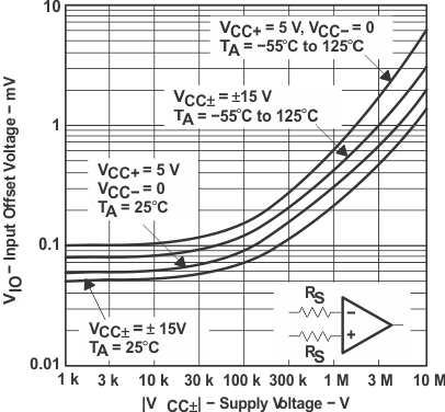 Figure 1. Input Offset Voltage vs Input Resistance
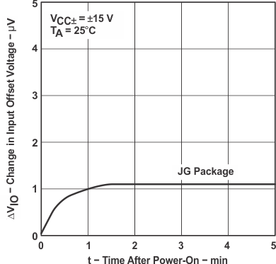 Figure 3. Warm-Up Change in Input Offset Voltage vs Time After Power On
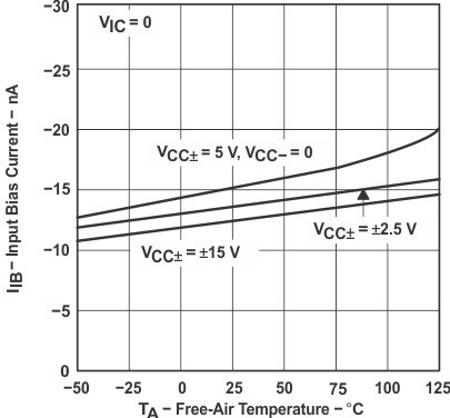 Figure 5. Input Bias Current vs Free-Air Temperature
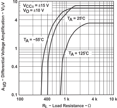 Figure 7. Differential Voltage Amplification vs Load Resistance
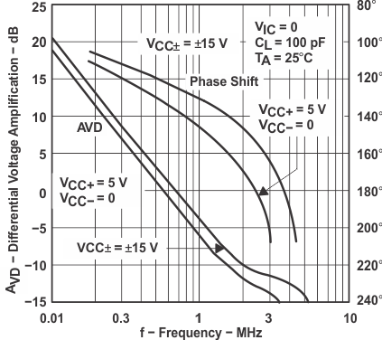 Figure 9. Differential Voltage Amplification and Phase Shift vs Frequency
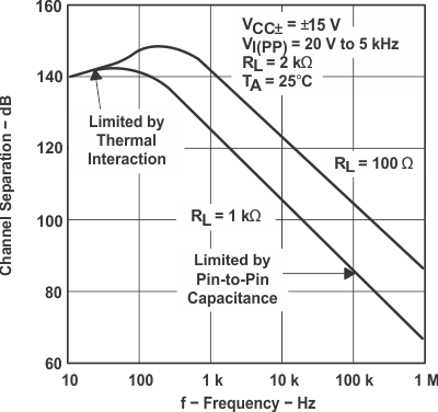 Figure 11. Channel Separation vs Frequency
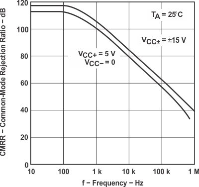 Figure 13. Common-Mode Rejection Ratio vs Frequency
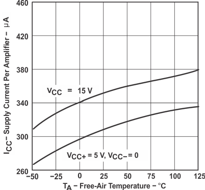 Figure 15. Supply Current vs Free-Air Temperature
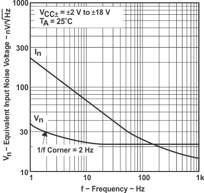 Figure 17. Equivalent Input Noise Voltage and Equivalent Input Noise Current vs Frequency
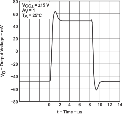 Figure 19. Voltage-Follower Small-Signal Pulse Response
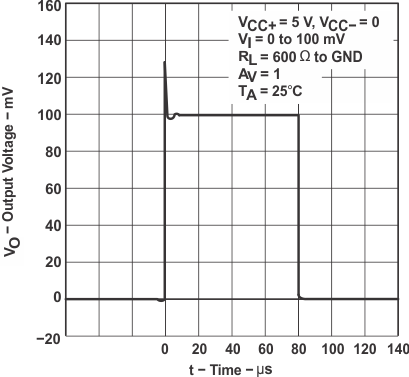 Figure 21. Voltage-Follower Small-Signal Pulse Response
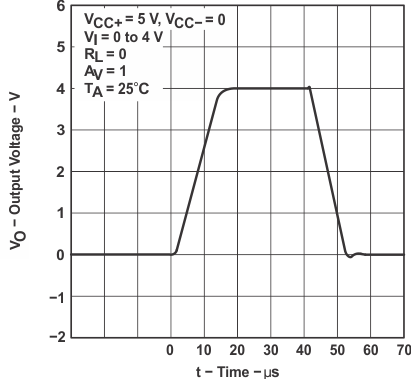 Figure 23. Voltage-Follower Large-Signal Pulse Response
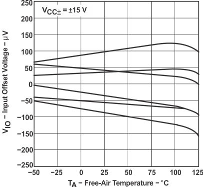 Figure 2. Input Offset Voltage of Representative Units vs Free-Air Temperature
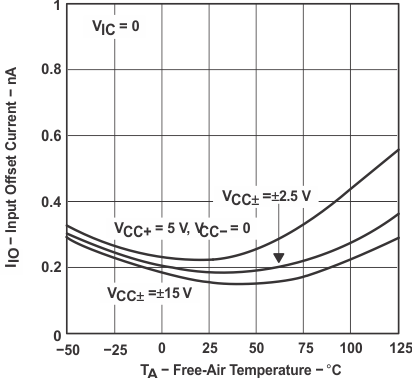 Figure 4. Input Offset Current vs Free-Air Temperature
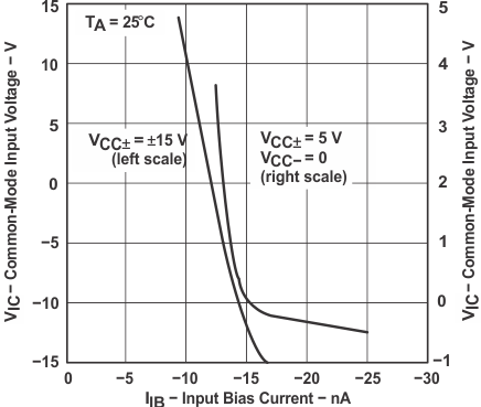 Figure 6. Common-Mode Input Voltage vs Input Bias Current
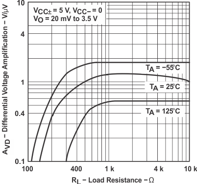 Figure 8. Differential Voltage Amplification vs Load Resistance
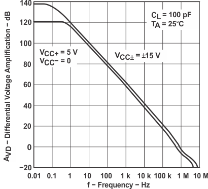 Figure 10. Differential Voltage Amplification vs Frequency
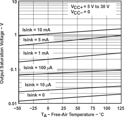 Figure 12. Output Saturation Voltage vs Free-Air Temperature
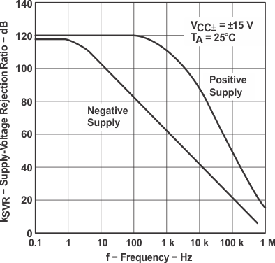 Figure 14. Supply-Voltage Rejection Ratio vs Frequency
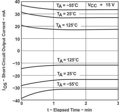 Figure 16. Short-Circuit Output Current vs Elapsed Time
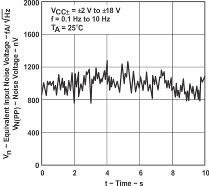 Figure 18. Peak-to-Peak Input Noise Voltage Over a
 10-Second Period
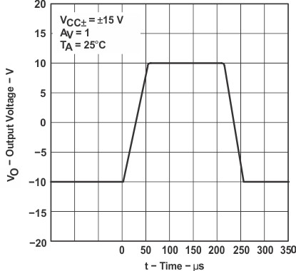 Figure 20. Voltage-Follower Large-Signal Pulse Response
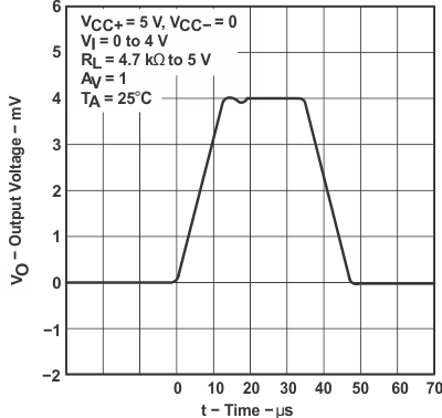 Figure 22. Voltage-Follower Large-Signal Pulse Response