SNVSA23B July   2014  – September 2023 LV284

PRODUCTION DATA  

  1.   1
  2. Features
  3. Applications
  4. Description
  5. Revision History
  6. Pin Configuration
  7. Specifications
    1. 6.1 Absolute Maximum Ratings
    2. 6.2 ESD Ratings
    3. 6.3 Recommended Operating Conditions
    4. 6.4 Thermal Information
    5. 6.5 Electrical Characteristics
    6. 6.6 Typical Characteristics
  8. Detailed Description
    1. 7.1 Overview
    2. 7.2 Functional Block Diagram
    3. 7.3 Feature Description
      1. 7.3.1 Fixed Frequency PWM Control
      2. 7.3.2 Bootstrap Voltage (CB)
      3. 7.3.3 Setting the Ouput Voltage
      4. 7.3.4 Enable (SHDN) and VIN Undervoltage Lockout
      5. 7.3.5 Current Limit
      6. 7.3.6 Thermal Shutdown
    4. 7.4 Device Functional Modes
      1. 7.4.1 Continuous Conduction Mode
      2. 7.4.2 Eco-mode
  9. Application and Implementation
    1. 8.1 Application Information
    2. 8.2 Typical Applications
      1. 8.2.1 5 V Output Application
        1. 8.2.1.1 Design Requirements
          1. 8.2.1.1.1 Design Guide – Step By Step Design Procedure
        2. 8.2.1.2 Detailed Design Procedure
          1. 8.2.1.2.1 Output Inductor Selection
          2. 8.2.1.2.2 Output Capacitor Selection
          3. 8.2.1.2.3 Schottky Diode Selection
          4. 8.2.1.2.4 Input Capacitor Selection
          5. 8.2.1.2.5 Bootstrap Capacitor Selection
        3. 8.2.1.3 Application Performance Curves
    3. 8.3 Power Supply Recommendations
    4. 8.4 Layout
      1. 8.4.1 Layout Guidelines
      2. 8.4.2 Layout Example
  10. Device and Documentation Support
    1. 9.1 Receiving Notification of Documentation Updates
    2. 9.2 Support Resources
    3. 9.3 Trademarks
    4. 9.4 Electrostatic Discharge Caution
    5. 9.5 Glossary
  11. 10Mechanical, Packaging, and Orderable Information

Package Options

Mechanical Data (Package|Pins)
Thermal pad, mechanical data (Package|Pins)
Orderable Information

Description

The LV284 is a PWM DC/DC buck (step-down) regulator. With a wide input range from 4 V to 40 V, the device is designed for a wide range of applications from industrial to automotive. An ultra-low, 1-µA shutdown current prolongs battery life. Operating frequency is fixed at 0.7 MHz allowing the use of small external components while still being able to have low output ripple voltage. Soft-start and compensation circuits are implemented internally, and these allow the device to be used with minimum external components.

The LV284 is optimized for up to 1-A load current. The device has a 0.765-V nominal feedback voltage.

The device has built-in protection features such as pulse-by-pulse current limit, thermal sensing and shutdown due to excessive power dissipation. The LV284 is available in a low profile TSOT-6L package (2.9 mm × 1.6 mm × 0.85 mm).
Package Information
PART NUMBER PACKAGE(1) PACKAGE SIZE(2)
LV284 DDC (TSOT-6L, 6) 2.90 mm × 2.80 mm
For all available packages, see the orderable addendum at the end of the data sheet.
The package size (length × width) is a nominal value and includes pins, where applicable.
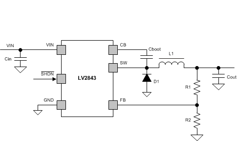
GUID-7AB344C2-83D4-4A63-A71E-8A0D7A47FB29-low.gifSimplified Schematic
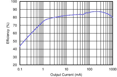
GUID-5ABCDA5D-A069-455D-BE97-7C8A9E6064DC-low.pngFigure 3-1 Efficiency vs. Current
SW= 0.7 MHz, VIN = 12 V, VOUT = 3.3 V)