SLLS567F May 2003 – July 2024 MAX211
PRODUCTION DATA
- 1
- 1 Features
- 2 Applications
- 3 Description
- 4 Pin Configuration and Functions
- 5 Specifications
- 6 Parameter Measurement Information
- 7 Device Functional Modes
- 8 Application and Implementation
- 9 Device and Documentation Support
- 10Revision History
- 11Mechanical, Packaging, and Orderable Information
Package Options
Refer to the PDF data sheet for device specific package drawings
Mechanical Data (Package|Pins)
- DB|28
- DW|28
Thermal pad, mechanical data (Package|Pins)
Orderable Information
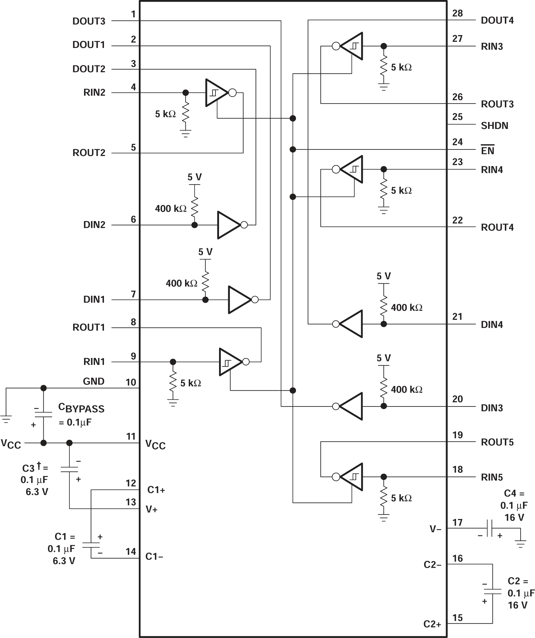
8.1 Application Information

Note: C3 can be connected to VCC or GND.
A. Resistor values shown are nominal.
B. Nonpolarized
ceramic capacitors are acceptable. If polarized tantalum or electrolytic
capacitors are used, connect the capacitors as shown.
Figure 8-1 Typical Operating Circuit and
Capacitor Values