SLLS348P June 1999 – July 2021 MAX3221
PRODUCTION DATA
- 1 Features
- 2 Applications
- 3 Description
- 4 Revision History
- 5 Pin Configuration and Functions
-
6 Specifications
- 6.1 Absolute Maximum Ratings
- 6.2 ESD Ratings
- 6.3 Recommended Operating Conditions
- 6.4 Thermal Information
- 6.5 Electrical Characteristics – Power
- 6.6 Electrical Characteristics – Driver
- 6.7 Electrical Characteristics – Receiver
- 6.8 Electrical Characteristics – Status
- 6.9 Switching Characteristics – Driver
- 6.10 Switching Characteristics – Receiver
- 6.11 Switching Characteristics – Status
- 6.12 Typical Characteristics
- 7 Parameter Measurement Information
- 8 Detailed Description
- 9 Application and Implementation
- 10Power Supply Recommendations
- 11Layout
- 12Device and Documentation Support
- 13Mechanical, Packaging, and Orderable Information
Package Options
Refer to the PDF data sheet for device specific package drawings
Mechanical Data (Package|Pins)
- DB|16
- PW|16
Thermal pad, mechanical data (Package|Pins)
Orderable Information
8.4 Device Functional Modes
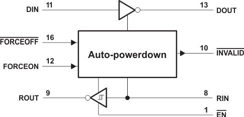
Table 8-1, Table 8-2, and Table 8-3 show the behavior of the driver, receiver, and INVALID(activelow) features under all possible relevant combinations of inputs.
Table 8-1 Driver(1)
| INPUTS | OUTPUT | DRIVER STATUS | |||
|---|---|---|---|---|---|
| DIN | FORCEON | FORCEOFF | VALID RIN RS-232 LEVEL | DOUT | |
| X | X | L | X | Z | Powered off |
| L | H | H | X | H | Normal operation with automatic power down disabled |
| H | H | H | X | L | |
| L | L | H | Yes | H | Normal operation with automatic power down enabled |
| H | L | H | Yes | L | |
| L | L | H | No | Z | Powered off by automatic power down feature |
| H | L | H | No | Z | |
(1) H = high level, L = low level, X = irrelevant, Z = high impedance, Yes = |RIN| > 2.7 V, No = |RIN| <0.3 V
Table 8-2 Receiver(1)
| INPUTS | OUTPUT | RECEIVER STATUS | ||
|---|---|---|---|---|
| RIN | EN | VALID RIN RS-232 LEVEL | ROUT | |
| X | H | X | Z | Output off |
| L | L | X | H | Normal operation |
| H | L | X | L | |
| Open | L | No | H | |
(1) H = high level, L = low level, X = irrelevant, Z = high impedance (off), Open = input disconnected or connected driver off
Table 8-3 INVALID(1)
| INPUTS | OUTPUT | |||
|---|---|---|---|---|
| RIN | FORCEON | FORCEOFF | EN | INVALID |
| L | X | X | X | H |
| H | X | X | X | H |
| Open | X | X | X | L |
(1) H = high level, L = low level, X = irrelevant, Z = high impedance (off), Open = input disconnected or connected driver off
 Figure 8-1 Logic Diagram