SLLS676B December 2005 – December 2024 MAX3232E-Q1
PRODUCTION DATA
- 1
- 1Features
- 2Applications
- 3Description
- 4Pin Configuration and Functions
-
5Specifications
- 5.1 Absolute Maximum Ratings
- 5.2 Recommended Operating Conditions
- 5.3 Thermal Information
- 5.4 Electrical Characteristics
- 5.5 Driver Section, Electrical Characteristics
- 5.6 Driver Section, Switching Characteristics
- 5.7 Receiver Section, Electrical Characteristics
- 5.8 Receiver Section, Switching Characteristics
- Parameter Measurement Information
- 6Application and Implementation
- 7Device and Documentation Support
- 8Revision History
- 9Mechanical, Packaging, and Orderable Information
Package Options
Mechanical Data (Package|Pins)
- PW|16
Thermal pad, mechanical data (Package|Pins)
Orderable Information
3 Description
The MAX3232E device consists of two line drivers, two line receivers, and a dual charge-pump circuit with ±15kV IEC ESD protection pin to pin (serial-port connection pins, including GND). The device meets the requirements of TIA/EIA-232-F and provides the electrical interface between an asynchronous communication controller and the serial-port connector. The charge pump and four small external capacitors allow operation from a single 3V to 5.5V supply. The device operates at data signaling rates up to 250kbit/s and a maximum of 30V/μs driver output slew rate.
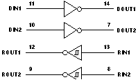
 Logic Diagram (Positive
Logic)