SLLSFU1A December   2023  – July 2024 MCF8315C

PRODMIX  

  1.   1
  2. Features
  3. Applications
  4. Description
  5. Pin Configuration and Functions
  6. Specifications
    1. 5.1 Absolute Maximum Ratings
    2. 5.2 ESD Ratings
    3. 5.3 Recommended Operating Conditions
    4. 5.4 Thermal Information
    5. 5.5 Electrical Characteristics
    6. 5.6 Characteristics of the SDA and SCL bus for Standard and Fast mode
  7. Detailed Description
    1. 6.1 Overview
    2. 6.2 Functional Block Diagram
    3. 6.3 Feature Description
      1. 6.3.1  Output Stage
      2. 6.3.2  Device Interface
        1. 6.3.2.1 Interface - Control and Monitoring
        2. 6.3.2.2 I2C Interface
      3. 6.3.3  Step-Down Mixed-Mode Buck Regulator
        1. 6.3.3.1 Buck in Inductor Mode
        2. 6.3.3.2 Buck in Resistor mode
        3. 6.3.3.3 Buck Regulator with External LDO
        4. 6.3.3.4 AVDD Power Sequencing from Buck Regulator
        5. 6.3.3.5 Mixed Mode Buck Operation and Control
        6. 6.3.3.6 Buck Under Voltage Protection
        7. 6.3.3.7 Buck Over Current Protection
      4. 6.3.4  AVDD Linear Voltage Regulator
      5. 6.3.5  Charge Pump
      6. 6.3.6  Slew Rate Control
      7. 6.3.7  Cross Conduction (Dead Time)
      8. 6.3.8  Motor Control Input Sources
        1. 6.3.8.1 Analog Mode Motor Control
        2. 6.3.8.2 PWM Mode Motor Control
        3. 6.3.8.3 I2C based Motor Control
        4. 6.3.8.4 Frequency Mode Motor Control
        5. 6.3.8.5 Speed Profiles
          1. 6.3.8.5.1 Linear Reference Profiles
          2. 6.3.8.5.2 Staircase Reference Profiles
          3. 6.3.8.5.3 Forward-Reverse Reference Profiles
      9. 6.3.9  Starting the Motor Under Different Initial Conditions
        1. 6.3.9.1 Case 1 – Motor is Stationary
        2. 6.3.9.2 Case 2 – Motor is Spinning in the Forward Direction
        3. 6.3.9.3 Case 3 – Motor is Spinning in the Reverse Direction
      10. 6.3.10 Motor Start Sequence (MSS)
        1. 6.3.10.1 Initial Speed Detect (ISD)
        2. 6.3.10.2 Motor Resynchronization
        3. 6.3.10.3 Reverse Drive
          1. 6.3.10.3.1 Reverse Drive Tuning
      11. 6.3.11 Motor Start-up
        1. 6.3.11.1 Align
        2. 6.3.11.2 Double Align
        3. 6.3.11.3 Initial Position Detection (IPD)
          1. 6.3.11.3.1 IPD Operation
          2. 6.3.11.3.2 IPD Release Mode
          3. 6.3.11.3.3 IPD Advance Angle
        4. 6.3.11.4 Slow First Cycle Start-up
        5. 6.3.11.5 Open loop
        6. 6.3.11.6 Transition from Open to Closed Loop
      12. 6.3.12 Closed Loop Operation
        1. 6.3.12.1 Closed Loop Acceleration/Deceleration Slew Rate
        2. 6.3.12.2 Speed PI Control
        3. 6.3.12.3 Current PI Control
        4. 6.3.12.4 Torque Mode
        5. 6.3.12.5 Overmodulation
      13. 6.3.13 Motor Parameters
        1. 6.3.13.1 Motor Resistance
        2. 6.3.13.2 Motor Inductance
        3. 6.3.13.3 Motor Back-EMF constant
      14. 6.3.14 Motor Parameter Extraction Tool (MPET)
      15. 6.3.15 Anti-Voltage Surge (AVS)
      16. 6.3.16 Active Braking
      17. 6.3.17 Output PWM Switching Frequency
      18. 6.3.18 PWM Modulation Schemes
      19. 6.3.19 Dead Time Compensation
      20. 6.3.20 Motor Stop Options
        1. 6.3.20.1 Coast (Hi-Z) Mode
        2. 6.3.20.2 Low-Side Braking
        3. 6.3.20.3 Active Spin-Down
      21. 6.3.21 FG Configuration
        1. 6.3.21.1 FG Output Frequency
        2. 6.3.21.2 FG during open loop
        3. 6.3.21.3 FG during idle and fault
      22. 6.3.22 DC Bus Current Limit
      23. 6.3.23 Protections
        1. 6.3.23.1  VM Supply Undervoltage Lockout
        2. 6.3.23.2  AVDD Undervoltage Lockout (AVDD_UV)
        3. 6.3.23.3  BUCK Under Voltage Lockout (BUCK_UV)
        4. 6.3.23.4  VCP Charge Pump Undervoltage Lockout (CPUV)
        5. 6.3.23.5  Overvoltage Protection (OVP)
        6. 6.3.23.6  Overcurrent Protection (OCP)
          1. 6.3.23.6.1 OCP Latched Shutdown (OCP_MODE = 00b)
          2. 6.3.23.6.2 OCP Automatic Retry (OCP_MODE = 01b)
        7. 6.3.23.7  Buck Overcurrent Protection
        8. 6.3.23.8  Hardware Lock Detection Current Limit (HW_LOCK_ILIMIT)
          1. 6.3.23.8.1 HW_LOCK_ILIMIT Latched Shutdown (HW_LOCK_ILIMIT_MODE = 00xxb)
          2. 6.3.23.8.2 HW_LOCK_ILIMIT Automatic recovery (HW_LOCK_ILIMIT_MODE = 01xxb)
          3. 6.3.23.8.3 HW_LOCK_ILIMIT Report Only (HW_LOCK_ILIMIT_MODE = 1000b)
          4. 6.3.23.8.4 HW_LOCK_ILIMIT Disabled (HW_LOCK_ILIMIT_MODE= 1xx1b)
        9. 6.3.23.9  Motor Lock (MTR_LCK)
          1. 6.3.23.9.1 MTR_LCK Latched Shutdown (MTR_LCK_MODE = 00xxb)
          2. 6.3.23.9.2 MTR_LCK Automatic Recovery (MTR_LCK_MODE= 01xxb)
          3. 6.3.23.9.3 MTR_LCK Report Only (MTR_LCK_MODE = 1000b)
          4. 6.3.23.9.4 MTR_LCK Disabled (MTR_LCK_MODE = 1xx1b)
        10. 6.3.23.10 Motor Lock Detection
          1. 6.3.23.10.1 Lock 1: Abnormal Speed (ABN_SPEED)
          2. 6.3.23.10.2 Lock 2: Abnormal BEMF (ABN_BEMF)
          3. 6.3.23.10.3 Lock3: No-Motor Fault (NO_MTR)
        11. 6.3.23.11 Minimum VM (undervoltage) Protection
        12. 6.3.23.12 Maximum VM (overvoltage) Protection
        13. 6.3.23.13 MPET Faults
        14. 6.3.23.14 IPD Faults
        15. 6.3.23.15 Thermal Warning (OTW)
        16. 6.3.23.16 Thermal Shutdown (TSD)
    4. 6.4 Device Functional Modes
      1. 6.4.1 Functional Modes
        1. 6.4.1.1 Sleep Mode
        2. 6.4.1.2 Standby Mode
        3. 6.4.1.3 Fault Reset (CLR_FLT)
    5. 6.5 External Interface
      1. 6.5.1 DRVOFF Functionality
      2. 6.5.2 DAC output
      3. 6.5.3 Oscillator Source
        1. 6.5.3.1 External Clock Source
      4. 6.5.4 External Watchdog
    6. 6.6 EEPROM access and I2C interface
      1. 6.6.1 EEPROM Access
        1. 6.6.1.1 EEPROM Write
        2. 6.6.1.2 EEPROM Read
      2. 6.6.2 I2C Serial Interface
        1. 6.6.2.1 I2C Data Word
        2. 6.6.2.2 I2C Write Transaction
        3. 6.6.2.3 I2C Read Transaction
        4. 6.6.2.4 I2C Communication Protocol Packet Examples
        5. 6.6.2.5 I2C Clock Stretching
        6. 6.6.2.6 CRC Byte Calculation
  8. EEPROM (Non-Volatile) Register Map
    1. 7.1 Algorithm_Configuration Registers
    2. 7.2 Fault_Configuration Registers
    3. 7.3 Hardware_Configuration Registers
    4. 7.4 Internal_Algorithm_Configuration Registers
  9. RAM (Volatile) Register Map
    1. 8.1 Fault_Status Registers
    2. 8.2 System_Status Registers
    3. 8.3 Device_Control Registers
    4. 8.4 Algorithm_Control Registers
    5. 8.5 Algorithm_Variables Registers
  10. Application and Implementation
    1. 9.1 Application Information
    2. 9.2 Typical Applications
      1. 9.2.1 Application Curves
        1. 9.2.1.1 Motor startup
        2. 9.2.1.2 MPET
        3. 9.2.1.3 Dead time compensation
        4. 9.2.1.4 Auto handoff
        5. 9.2.1.5 Anti voltage surge (AVS)
    3. 9.3 Power Supply Recommendations
      1. 9.3.1 Bulk Capacitance
    4. 9.4 Layout
      1. 9.4.1 Layout Guidelines
      2. 9.4.2 Thermal Considerations
        1. 9.4.2.1 Power Dissipation
  11. 10Device and Documentation Support
    1. 10.1 Support Resources
    2. 10.2 Trademarks
    3. 10.3 Electrostatic Discharge Caution
    4. 10.4 Glossary
  12. 11Revision History
  13. 12Mechanical, Packaging, and Orderable Information

Package Options

Mechanical Data (Package|Pins)
Thermal pad, mechanical data (Package|Pins)
Orderable Information

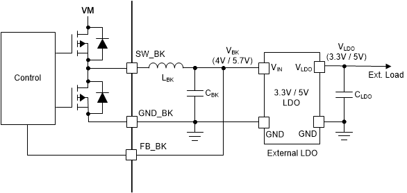
Buck Regulator with External LDO

The buck regulator also supports the voltage requirement to supply an external LDO to generate standard 3.3V or 5V output rail with higher accuracies. The buck output voltage should be configured to 4V or 5.7V to provide extra headroom to support the external LDO for generating 3.3V or 5V rail as shown in Figure 6-5. This allows for a lower-voltage LDO design to save cost and better thermal management due to low drop-out voltage.
MCF8315C Buck Regulator with External LDOFigure 6-5 Buck Regulator with External LDO