SLVSH86A December   2023  – June 2024 MCT8314Z

PRODUCTION DATA  

  1.   1
  2. Features
  3. Applications
  4. Description
  5. Device Comparison Table
  6. Pin Configuration and Functions
  7. Specifications
    1. 6.1 Absolute Maximum Ratings
    2. 6.2 ESD Ratings
    3. 6.3 Recommended Operating Conditions
    4. 6.4 Thermal Information
    5. 6.5 Electrical Characteristics
    6. 6.6 SPI Timing Requirements
    7. 6.7 SPI Secondary Device Mode Timings
    8. 6.8 Typical Characteristics
  8. Detailed Description
    1. 7.1 Overview
    2. 7.2 Functional Block Diagram
    3. 7.3 Feature Description
      1. 7.3.1  Output Stage
      2. 7.3.2  PWM Control Mode (1x PWM Mode)
        1. 7.3.2.1 Analog Hall Input Configuration
        2. 7.3.2.2 Digital Hall Input Configuration
        3. 7.3.2.3 Asynchronous Modulation
        4. 7.3.2.4 Synchronous Modulation
        5. 7.3.2.5 Motor Operation
      3. 7.3.3  Device Interface Modes
        1. 7.3.3.1 Serial Peripheral Interface (SPI)
        2. 7.3.3.2 Hardware Interface
      4. 7.3.4  AVDD Linear Voltage Regulator
      5. 7.3.5  Charge Pump
      6. 7.3.6  Slew Rate
      7. 7.3.7  Cross Conduction (Dead Time)
      8. 7.3.8  Propagation Delay
      9. 7.3.9  Pin Diagrams
        1. 7.3.9.1 Logic Level Input Pin (Internal Pulldown)
        2. 7.3.9.2 Logic Level Input Pin (Internal Pullup)
        3. 7.3.9.3 Open Drain Pin
        4. 7.3.9.4 Push Pull Pin
        5. 7.3.9.5 Seven Level Input Pin
      10. 7.3.10 Automatic Synchronous Rectification Mode (ASR Mode)
      11. 7.3.11 Cycle-by-Cycle Current Limit
        1. 7.3.11.1 Cycle by Cycle Current Limit with 100% Duty Cycle Input
      12. 7.3.12 Hall Comparators (Analog Hall Inputs)
      13. 7.3.13 Advance Angle
      14. 7.3.14 FG Signal
      15. 7.3.15 Protections
        1. 7.3.15.1 VM Supply Undervoltage Lockout (NPOR)
        2. 7.3.15.2 AVDD Undervoltage Lockout (AVDD_UV)
        3. 7.3.15.3 VCP Charge Pump Undervoltage Lockout (CPUV)
        4. 7.3.15.4 Overvoltage Protections (OVP)
        5. 7.3.15.5 Overcurrent Protection (OCP)
          1. 7.3.15.5.1 OCP Latched Shutdown (OCP_MODE = 00b or MCT8314ZH)
          2. 7.3.15.5.2 OCP Automatic Retry (OCP_MODE = 01b)
          3. 7.3.15.5.3 OCP Report Only (OCP_MODE = 10b)
          4. 7.3.15.5.4 OCP Disabled (OCP_MODE = 11b)
        6. 7.3.15.6 Motor Lock (MTR_LOCK)
          1. 7.3.15.6.1 MTR_LOCK Latched Shutdown (MTR_LOCK_MODE = 00b)
          2. 7.3.15.6.2 MTR_LOCK Automatic Retry (MTR_LOCK_MODE = 01b or MCT8314ZH)
          3. 7.3.15.6.3 MTR_LOCK Report Only (MTR_LOCK_MODE= 10b)
          4. 7.3.15.6.4 MTR_LOCK Disabled (MTR_LOCK_MODE = 11b)
        7. 7.3.15.7 Thermal Warning (OTW)
        8. 7.3.15.8 Thermal Shutdown (OTS)
    4. 7.4 Device Functional Modes
      1. 7.4.1 Functional Modes
        1. 7.4.1.1 Sleep Mode
        2. 7.4.1.2 Operating Mode
        3. 7.4.1.3 Fault Reset (CLR_FLT or nSLEEP Reset Pulse)
    5. 7.5 SPI Communication
      1. 7.5.1 Programming
        1. 7.5.1.1 SPI Format
  9. Register Map
    1. 8.1 STATUS Registers
    2. 8.2 CONTROL Registers
  10. Application and Implementation
    1. 9.1 Application Information
    2. 9.2 Hall Sensor Configuration and Connection
      1. 9.2.1 Typical Configuration
      2. 9.2.2 Open Drain Configuration
      3. 9.2.3 Series Configuration
      4. 9.2.4 Parallel Configuration
    3. 9.3 Typical Applications
      1. 9.3.1 Three-Phase Brushless-DC Motor Control With Current Limit
        1. 9.3.1.1 Detailed Design Procedure
          1. 9.3.1.1.1 Motor Voltage
          2. 9.3.1.1.2 Using Automatic Synchronous Rectification Mode (ASR Mode)
          3. 9.3.1.1.3 Power Dissipation and Junction Temperature Losses
        2. 9.3.1.2 Application Curves
    4. 9.4 Power Supply Recommendations
      1. 9.4.1 Bulk Capacitance
    5. 9.5 Layout
      1. 9.5.1 Layout Guidelines
      2. 9.5.2 Layout Example
      3. 9.5.3 Thermal Considerations
        1. 9.5.3.1 Power Dissipation
  11. 10Device and Documentation Support
    1. 10.1 Documentation Support
      1. 10.1.1 Related Documentation
    2. 10.2 Support Resources
    3. 10.3 Trademarks
    4. 10.4 Electrostatic Discharge Caution
    5. 10.5 Glossary
  12. 11Revision History
  13. 12Mechanical, Packaging, and Orderable Information
    1. 12.1 Package Option Addendum
    2. 12.2 Tape and Reel Information

Package Options

Mechanical Data (Package|Pins)
Thermal pad, mechanical data (Package|Pins)
Orderable Information

Cycle-by-Cycle Current Limit

The current-limit circuit activates if the current flowing through the low-side MOSFETs exceeds the ILIMIT current. Large currents may occur during motor start, high torque events, or stall conditions. The current-limit circuitry utilizes the internal sense FETs on the low-side power FETs of the three phases. Figure 7-22 shows the implementation of current limit circuitry. The ILIM pin sets the ILIMIT by connecting an RLIMIT from ILIM to AGND. Equation 3 calculates the resistor value in Ohms required for a target ILIMIT threshold.

Equation 3. RLIMIT = 9000/ILIMIT

MCT8314Z Current Limit Implementation

Figure 7-22 Current Limit Implementation

When the current limit activates, the high-side FETs disable until the beginning of the next PWM cycle as shown in Figure 7-23. The low-side FETs can operate in brake mode or coast (high-Z) mode by configuring the ILIM_RECIR bit in the SPI device variant. In the hardware device, the device operates in brake mode when current limiting trips.
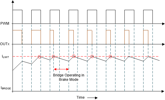
MCT8314Z Cycle-by-Cycle Current-Limit
                    Operation Figure 7-23 Cycle-by-Cycle Current-Limit Operation

When the current limit activates in synchronous rectification mode, the current recirculates through the low-side FETs while the high-side FETs are disabled as shown in Figure 7-24. When the current limit activates in asynchronous rectification mode, the current recirculates through the body diodes of the low-side FETs while the high-side FETs are disabled as shown in Figure 7-25