SLVSH53 December   2023 MCT8315Z

PRODUCTION DATA  

  1.   1
  2. Features
  3. Applications
  4. Description
  5. Revision History
  6. Device Comparison Table
  7. Pin Configuration and Functions
  8. Specifications
    1. 7.1 Absolute Maximum Ratings
    2. 7.2 ESD Ratings
    3. 7.3 Recommended Operating Conditions
    4. 7.4 Thermal Information
    5. 7.5 Electrical Characteristics
    6. 7.6 SPI Timing Requirements
    7. 7.7 SPI Secondary Device Mode Timings
    8. 7.8 Typical Characteristics
  9. Detailed Description
    1. 8.1 Overview
    2. 8.2 Functional Block Diagram
    3. 8.3 Feature Description
      1. 8.3.1  Output Stage
      2. 8.3.2  PWM Control Mode (1x PWM Mode)
        1. 8.3.2.1 Analog Hall Input Configuration
        2. 8.3.2.2 Digital Hall Input Configuration
        3. 8.3.2.3 Asynchronous Modulation
        4. 8.3.2.4 Synchronous Modulation
        5. 8.3.2.5 Motor Operation
      3. 8.3.3  Device Interface Modes
        1. 8.3.3.1 Serial Peripheral Interface (SPI)
        2. 8.3.3.2 Hardware Interface
      4. 8.3.4  Step-Down Mixed-Mode Buck Regulator
        1. 8.3.4.1 Buck in Inductor Mode
        2. 8.3.4.2 Buck in Resistor mode
        3. 8.3.4.3 Buck Regulator with External LDO
        4. 8.3.4.4 AVDD Power Sequencing on Buck Regulator
        5. 8.3.4.5 Mixed mode Buck Operation and Control
      5. 8.3.5  AVDD Linear Voltage Regulator
      6. 8.3.6  Charge Pump
      7. 8.3.7  Slew Rate Control
      8. 8.3.8  Cross Conduction (Dead Time)
      9. 8.3.9  Propagation Delay
        1. 8.3.9.1 Driver Delay Compensation
      10. 8.3.10 Pin Diagrams
        1. 8.3.10.1 Logic Level Input Pin (Internal Pulldown)
        2. 8.3.10.2 Logic Level Input Pin (Internal Pullup)
        3. 8.3.10.3 Open Drain Pin
        4. 8.3.10.4 Push Pull Pin
        5. 8.3.10.5 Four Level Input Pin
        6. 8.3.10.6 Seven Level Input Pin
      11. 8.3.11 Active Demagnetization
        1. 8.3.11.1 Automatic Synchronous Rectification Mode (ASR Mode)
          1. 8.3.11.1.1 Automatic Synchronous Rectification in Commutation
          2. 8.3.11.1.2 Automatic Synchronous Rectification in PWM Mode
        2. 8.3.11.2 Automatic Asynchronous Rectification Mode (AAR Mode)
      12. 8.3.12 Cycle-by-Cycle Current Limit
        1. 8.3.12.1 Cycle by Cycle Current Limit with 100% Duty Cycle Input
      13. 8.3.13 Hall Comparators (Analog Hall Inputs)
      14. 8.3.14 Advance Angle
      15. 8.3.15 FGOUT Signal
      16. 8.3.16 Protections
        1. 8.3.16.1  VM Supply Undervoltage Lockout (NPOR)
        2. 8.3.16.2  AVDD Undervoltage Lockout (AVDD_UV)
        3. 8.3.16.3  Buck Undervoltage Lockout (BUCK_UV)
        4. 8.3.16.4  VCP Charge Pump Undervoltage Lockout (CPUV)
        5. 8.3.16.5  Overvoltage Protection (OVP)
        6. 8.3.16.6  Overcurrent Protection (OCP)
          1. 8.3.16.6.1 OCP Latched Shutdown (OCP_MODE = 00b)
          2. 8.3.16.6.2 OCP Automatic Retry (OCP_MODE = 01b)
        7. 8.3.16.7  Buck Overcurrent Protection
        8. 8.3.16.8  Motor Lock (MTR_LOCK)
          1. 8.3.16.8.1 MTR_LOCK Latched Shutdown (MTR_LOCK_MODE = 00b)
          2. 8.3.16.8.2 MTR_LOCK Automatic Retry (MTR_LOCK_MODE = 01b)
          3. 8.3.16.8.3 MTR_LOCK Report Only (MTR_LOCK_MODE= 10b)
          4. 8.3.16.8.4 MTR_LOCK Disabled (MTR_LOCK_MODE = 11b)
          5. 8.3.16.8.5 75
        9. 8.3.16.9  Thermal Warning (OTW)
        10. 8.3.16.10 Thermal Shutdown (OTSD)
          1. 8.3.16.10.1 OTSD FET
          2. 8.3.16.10.2 OTSD (Non-FET)
    4. 8.4 Device Functional Modes
      1. 8.4.1 Functional Modes
        1. 8.4.1.1 Sleep Mode
        2. 8.4.1.2 Operating Mode
        3. 8.4.1.3 Fault Reset (CLR_FLT or nSLEEP Reset Pulse)
      2. 8.4.2 DRVOFF
    5. 8.5 SPI Communication
      1. 8.5.1 Programming
        1. 8.5.1.1 SPI Format
    6. 8.6 Register Map
      1. 8.6.1 STATUS Registers
      2. 8.6.2 CONTROL Registers
  10. Application and Implementation
    1. 9.1 Application Information
    2. 9.2 Hall Sensor Configuration and Connection
      1. 9.2.1 Typical Configuration
      2. 9.2.2 Open Drain Configuration
      3. 9.2.3 Series Configuration
      4. 9.2.4 Parallel Configuration
    3. 9.3 Typical Applications
      1. 9.3.1 Three-Phase Brushless-DC Motor Control With Current Limit
        1. 9.3.1.1 Detailed Design Procedure
          1. 9.3.1.1.1 Motor Voltage
          2. 9.3.1.1.2 Using Active Demagnetization
          3. 9.3.1.1.3 Using Delay Compensation
          4. 9.3.1.1.4 Using the Buck Regulator
          5. 9.3.1.1.5 Power Dissipation and Junction Temperature Losses
        2. 9.3.1.2 Application Curves
  11. 10Power Supply Recommendations
    1. 10.1 Bulk Capacitance
  12. 11Layout
    1. 11.1 Layout Guidelines
    2. 11.2 Layout Example
    3. 11.3 Thermal Considerations
      1. 11.3.1 Power Dissipation
  13. 12Device and Documentation Support
    1. 12.1 Documentation Support
      1. 12.1.1 Related Documentation
    2. 12.2 Support Resources
    3. 12.3 Trademarks
    4. 12.4 Electrostatic Discharge Caution
    5. 12.5 Glossary
  14. 13Mechanical, Packaging, and Orderable Information

Package Options

Mechanical Data (Package|Pins)
Thermal pad, mechanical data (Package|Pins)
Orderable Information

Automatic Asynchronous Rectification Mode (AAR Mode)

Figure 8-34 shows the operation of AAR in PWM mode. As shown in this figure, a PWM is applied in a synchronous rectification to the high-side and low-side FETs. During the low-side FET conduction, for lower inductance motors, the current can decay to zero and becomes negative since low side FET is in on-state. This creates a negative torque on the BLDC motor operation. When AAR mode is enabled, the current during the decay is monitored and the low-side FET is turned off as soon as the current reaches near to zero. This saves the negative current building in the BLDC motor which results in better noise performance and better thermal management.
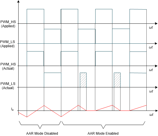
GUID-CFB80D83-9D21-4811-852B-55E178469749-low.gifFigure 8-34 AAR in PWM Mode