SLLSFQ3 January   2023 MCT8329A

PRODUCTION DATA  

  1. Features
  2. Applications
  3. Description
  4. Revision History
  5. Pin Configuration and Functions
  6. Specifications
    1. 6.1 Absolute Maximum Ratings
    2. 6.2 ESD Ratings Comm
    3. 6.3 Recommended Operating Conditions
    4. 6.4 Thermal Information 1pkg
    5. 6.5 Electrical Characteristics
    6. 6.6 Characteristics of the SDA and SCL bus for Standard and Fast mode
    7. 6.7 Typical Characteristics
  7. Detailed Description
    1. 7.1 Overview
    2. 7.2 Functional Block Diagram
    3. 7.3 Feature Description
      1. 7.3.1  Three Phase BLDC Gate Drivers
      2. 7.3.2  Gate Drive Architecture
        1. 7.3.2.1 Dead time and Cross Conduction Prevention
      3. 7.3.3  AVDD Linear Voltage Regulator
      4. 7.3.4  DVDD Voltage Regulator
        1. 7.3.4.1 AVDD Powered VREG
        2. 7.3.4.2 External Supply for VREG
        3. 7.3.4.3 External MOSFET for VREG Supply
      5. 7.3.5  Low-Side Current Sense Amplifier
      6. 7.3.6  Device Interface Modes
        1. 7.3.6.1 Interface - Control and Monitoring
        2. 7.3.6.2 I2C Interface
      7. 7.3.7  Motor Control Input Options
        1. 7.3.7.1 Analog-Mode Motor Control
        2. 7.3.7.2 PWM-Mode Motor Control
        3. 7.3.7.3 Frequency-Mode Motor Control
        4. 7.3.7.4 I2C based Motor Control
        5. 7.3.7.5 Input Control Signal Profiles
          1. 7.3.7.5.1 Linear Control Profiles
          2. 7.3.7.5.2 Staircase Control Profiles
          3. 7.3.7.5.3 Forward-Reverse Profiles
        6. 7.3.7.6 Control Input Transfer Function without Profiler
      8. 7.3.8  Starting the Motor Under Different Initial Conditions
        1. 7.3.8.1 Case 1 – Motor is Stationary
        2. 7.3.8.2 Case 2 – Motor is Spinning in the Forward Direction
        3. 7.3.8.3 Case 3 – Motor is Spinning in the Reverse Direction
      9. 7.3.9  Motor Start Sequence (MSS)
        1. 7.3.9.1 Initial Speed Detect (ISD)
        2. 7.3.9.2 Motor Resynchronization
        3. 7.3.9.3 Reverse Drive
        4. 7.3.9.4 Motor Start-up
          1. 7.3.9.4.1 Align
          2. 7.3.9.4.2 Double Align
          3. 7.3.9.4.3 Initial Position Detection (IPD)
            1. 7.3.9.4.3.1 IPD Operation
            2. 7.3.9.4.3.2 IPD Release
            3. 7.3.9.4.3.3 IPD Advance Angle
          4. 7.3.9.4.4 Slow First Cycle Startup
          5. 7.3.9.4.5 Open loop
          6. 7.3.9.4.6 Transition from Open to Closed Loop
      10. 7.3.10 Closed Loop Operation
        1. 7.3.10.1 120o Commutation
          1. 7.3.10.1.1 High-Side Modulation
          2. 7.3.10.1.2 Low-Side Modulation
          3. 7.3.10.1.3 Mixed Modulation
        2. 7.3.10.2 Variable Commutation
        3. 7.3.10.3 Lead Angle Control
        4. 7.3.10.4 Closed loop accelerate
      11. 7.3.11 Speed Loop
      12. 7.3.12 Power Loop
      13. 7.3.13 Anti-Voltage Surge (AVS)
      14. 7.3.14 Output PWM Switching Frequency
      15. 7.3.15 Fast Start-up (< 50 ms)
        1. 7.3.15.1 BEMF Threshold
        2. 7.3.15.2 Dynamic Degauss
      16. 7.3.16 Fast Deceleration
      17. 7.3.17 Dynamic Voltage Scaling
      18. 7.3.18 Motor Stop Options
        1. 7.3.18.1 Coast (Hi-Z) Mode
        2. 7.3.18.2 Recirculation Mode
        3. 7.3.18.3 Low-Side Braking
        4. 7.3.18.4 High-Side Braking
        5. 7.3.18.5 Active Spin-Down
      19. 7.3.19 FG Configuration
        1. 7.3.19.1 FG Output Frequency
        2. 7.3.19.2 FG in Open-Loop
        3. 7.3.19.3 FG During Motor Stop
        4. 7.3.19.4 FG Behaviour During Fault
      20. 7.3.20 Protections
        1. 7.3.20.1  PVDD Supply Undervoltage Lockout (PVDD_UV)
        2. 7.3.20.2  AVDD Power on Reset (AVDD_POR)
        3. 7.3.20.3  GVDD Undervoltage Lockout (GVDD_UV)
        4. 7.3.20.4  BST Undervoltage Lockout (BST_UV)
        5. 7.3.20.5  MOSFET VDS Overcurrent Protection (VDS_OCP)
        6. 7.3.20.6  VSENSE Overcurrent Protection (SEN_OCP)
        7. 7.3.20.7  Thermal Shutdown (OTSD)
        8. 7.3.20.8  Cycle-by-Cycle (CBC) Current Limit (CBC_ILIMIT)
          1. 7.3.20.8.1 CBC_ILIMIT Automatic Recovery next PWM Cycle (CBC_ILIMIT_MODE = 000xb)
          2. 7.3.20.8.2 CBC_ILIMIT Automatic Recovery Threshold Based (CBC_ILIMIT_MODE = 001xb)
          3. 7.3.20.8.3 CBC_ILIMIT Automatic Recovery after 'n' PWM Cycles (CBC_ILIMIT_MODE = 010xb)
          4. 7.3.20.8.4 CBC_ILIMIT Report Only (CBC_ILIMIT_MODE = 0110b)
          5. 7.3.20.8.5 CBC_ILIMIT Disabled (CBC_ILIMIT_MODE = 0111b or 1xxxb)
        9. 7.3.20.9  Lock Detection Current Limit (LOCK_ILIMIT)
          1. 7.3.20.9.1 LOCK_ILIMIT Latched Shutdown (LOCK_ILIMIT_MODE = 00xxb)
          2. 7.3.20.9.2 LOCK_ILIMIT Automatic Recovery (LOCK_ILIMIT_MODE = 01xxb)
          3. 7.3.20.9.3 LOCK_ILIMIT Report Only (LOCK_ILIMIT_MODE = 1000b)
          4. 7.3.20.9.4 LOCK_ILIMIT Disabled (LOCK_ILIMIT_MODE = 1xx1b)
        10. 7.3.20.10 Motor Lock (MTR_LCK)
          1. 7.3.20.10.1 MTR_LCK Latched Shutdown (MTR_LCK_MODE = 00xxb)
          2. 7.3.20.10.2 MTR_LCK Automatic Recovery (MTR_LCK_MODE= 01xxb)
          3. 7.3.20.10.3 MTR_LCK Report Only (MTR_LCK_MODE = 1000b)
          4. 7.3.20.10.4 MTR_LCK Disabled (MTR_LCK_MODE = 1xx1b)
        11. 7.3.20.11 Motor Lock Detection
          1. 7.3.20.11.1 Lock 1: Abnormal Speed (ABN_SPEED)
          2. 7.3.20.11.2 Lock 2: Loss of Sync (LOSS_OF_SYNC)
          3. 7.3.20.11.3 Lock3: No-Motor Fault (NO_MTR)
        12. 7.3.20.12 IPD Faults
    4. 7.4 Device Functional Modes
      1. 7.4.1 Functional Modes
        1. 7.4.1.1 Sleep Mode
        2. 7.4.1.2 Standby Mode
        3. 7.4.1.3 Fault Reset (CLR_FLT)
    5. 7.5 External Interface
      1. 7.5.1 DRVOFF - Gate Driver Shutdown Functionality
      2. 7.5.2 DAC outputs
      3. 7.5.3 Current Sense Amplifier Output
      4. 7.5.4 Oscillator Source
        1. 7.5.4.1 External Clock Source
    6. 7.6 EEPROM access and I2C interface
      1. 7.6.1 EEPROM Access
        1. 7.6.1.1 EEPROM Write
        2. 7.6.1.2 EEPROM Read
      2. 7.6.2 I2C Serial Interface
        1. 7.6.2.1 I2C Data Word
        2. 7.6.2.2 I2C Write Operation
        3. 7.6.2.3 I2C Read Operation
        4. 7.6.2.4 Examples of I2C Communication Protocol Packets
        5. 7.6.2.5 Internal Buffers
        6. 7.6.2.6 CRC Byte Calculation
    7. 7.7 EEPROM (Non-Volatile) Register Map
      1. 7.7.1 Algorithm_Configuration Registers
      2. 7.7.2 Fault_Configuration Registers
      3. 7.7.3 Hardware_Configuration Registers
      4. 7.7.4 Gate_Driver_Configuration Registers
    8. 7.8 RAM (Volatile) Register Map
      1. 7.8.1 Fault_Status Registers
      2. 7.8.2 System_Status Registers
      3. 7.8.3 Algo_Control Registers
      4. 7.8.4 Device_Control Registers
      5. 7.8.5 Algorithm_Variables Registers
  8. Application and Implementation
    1. 8.1 Application Information
    2. 8.2 Typical Applications
      1.      Detailed Design Procedure
      2.      Bootstrap Capacitor and GVDD Capacitor Selection
      3. 8.2.1 Selection of External MOSFET for VREG Power Supply
      4.      Gate Drive Current
      5.      Gate Resistor Selection
      6.      System Considerations in High Power Designs
      7.      Capacitor Voltage Ratings
      8.      External Power Stage Components
      9. 8.2.2 Application curves
        1. 8.2.2.1 Motor startup
        2. 8.2.2.2 120o and variable commutation
        3. 8.2.2.3 Faster startup time
        4. 8.2.2.4 Setting the BEMF threshold
        5. 8.2.2.5 Maximum speed
        6. 8.2.2.6 Faster deceleration
  9. Power Supply Recommendations
    1. 9.1 Bulk Capacitance
  10. 10Layout
    1. 10.1 Layout Guidelines
    2. 10.2 Layout Example
    3. 10.3 Thermal Considerations
      1. 10.3.1 Power Dissipation
  11. 11Device and Documentation Support
    1. 11.1 Documentation Support
      1. 11.1.1 Related Documentation
    2. 11.2 Support Resources
    3. 11.3 Trademarks
    4. 11.4 Electrostatic Discharge Caution
    5. 11.5 Glossary
  12. 12Mechanical, Packaging, and Orderable Information

Package Options

Mechanical Data (Package|Pins)
Thermal pad, mechanical data (Package|Pins)
Orderable Information

Bulk Capacitance

Having an appropriate local bulk capacitance is an important factor in motor drive system design. It is generally beneficial to have more bulk capacitance, while the disadvantages are increased cost and physical size.

The amount of local capacitance needed depends on a variety of factors, including:

  • The highest current required by the motor system
  • The capacitance and current capability of the power supply
  • The amount of parasitic inductance between the power supply and motor system
  • The acceptable voltage ripple
  • The type of motor used (brushed DC, brushless DC, stepper)
  • The motor braking method

The inductance between the power supply and the motor drive system limits the rate at which current can change from the power supply. If the local bulk capacitance is too small, the system responds to excessive current demands or dumps from the motor with a change in PVDD voltage. When adequate bulk capacitance is used, the PVDD voltage remains stable and high current can be quickly supplied.

The data sheet generally provides a recommended value, but system-level testing is required to determine the appropriate bulk capacitor. The voltage rating for bulk capacitors should be higher than the operating voltage, to provide margin for cases when the motor transfers energy to the supply.
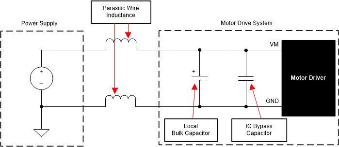
GUID-6CB3ED1C-0FE3-454A-B691-426AB59366F4-low.gifFigure 9-1 Example Setup of Motor Drive System With External Power Supply