SLAS272H July 2000 – May 2018 MSP430F133 , MSP430F135 , MSP430F147 , MSP430F1471 , MSP430F148 , MSP430F1481 , MSP430F149 , MSP430F1491
PRODUCTION DATA.
- 1Device Overview
- 2Revision History
- 3Device Comparison
- 4Terminal Configuration and Functions
-
5Specifications
- 5.1 Absolute Maximum Ratings
- 5.2 ESD Ratings
- 5.3 Recommended Operating Conditions
- 5.4 Supply Current Into AVCC and DVCC Excluding External Current
- 5.5 Thermal Resistance Characteristics
- 5.6 Schmitt-Trigger Inputs – Ports P1, P2, P3, P4, P5, and P6
- 5.7 Standard Inputs – RST/NMI, JTAG (TCK, TMS, TDI/TCLK, TDO/TDI)
- 5.8 Inputs – Px.y, TAx, TBx
- 5.9 Leakage Current
- 5.10 Outputs – Ports P1, P2, P3, P4, P5, and P6
- 5.11 Output Frequency
- 5.12 Typical Characteristics – Ports P1, P2, P3, P4, P5, and P6 Outputs
- 5.13 Wake-up Time From LPM3
- 5.14 RAM
- 5.15 Comparator_A
- 5.16 Typical Characteristics – Comparator_A
- 5.17 PUC and POR
- 5.18 DCO Frequency
- 5.19 DCO When Using ROSC
- 5.20 Crystal Oscillator, LFXT1
- 5.21 Crystal Oscillator, XT2
- 5.22 USART0, USART1
- 5.23 12-Bit ADC, Power Supply and Input Range Conditions
- 5.24 12-Bit ADC, External Reference
- 5.25 12-Bit ADC, Built-In Reference
- 5.26 12-Bit ADC, Timing Parameters
- 5.27 12-Bit ADC, Linearity Parameters
- 5.28 12-Bit ADC, Temperature Sensor and Built-In VMID
- 5.29 Flash Memory
- 5.30 JTAG Interface
- 5.31 JTAG Fuse
-
6Detailed Description
- 6.1 CPU
- 6.2 Instruction set
- 6.3 Operating Modes
- 6.4 Interrupt Vector Addresses
- 6.5 Bootloader (BSL)
- 6.6 JTAG Fuse Check Mode
- 6.7
Memory
- 6.7.1 Flash Memory
- 6.7.2
Special Function Registers
- Table 6-6 Interrupt Enable 1 Register Field Descriptions
- Table 6-7 Interrupt Enable 2 Register Field Descriptions
- Table 6-8 Interrupt Flag 1 Register Field Descriptions
- Table 6-9 Interrupt Flag 2 Register Field Descriptions
- Table 6-10 Module Enable 1 Bit Register Field Descriptions
- Table 6-11 Module Enable 2 Bit Register Field Descriptions
- 6.8
Peripherals
- 6.8.1 Digital I/O
- 6.8.2 Oscillator and System Clock
- 6.8.3 Watchdog Timer (WDT)
- 6.8.4 Hardware Multiplier (MSP430F14x and MSP430F14x1 Only)
- 6.8.5 USART0
- 6.8.6 USART1 (MSP430F14x and MSP430F14x1 Only)
- 6.8.7 Comparator_A
- 6.8.8 ADC12 (MSP430F14x and MSP430F13x Only)
- 6.8.9 Timer_A3
- 6.8.10 Timer_B3 (MSP430F13x Only)
- 6.8.11 Timer_B7 (MSP430F14x and MSP430F14x1 Only)
- 6.8.12 Peripheral File Map
- 6.9
Input/Output Diagrams
- 6.9.1 Port P1, Input/Output With Schmitt Trigger
- 6.9.2 Port P2, Input/Output With Schmitt Trigger
- 6.9.3 Port P3, Input/Output With Schmitt Trigger
- 6.9.4 Port P4, Input/Output With Schmitt Trigger
- 6.9.5 Port P5, Input/Output With Schmitt Trigger
- 6.9.6 Port P6, Input/Output With Schmitt Trigger
- 6.9.7 Port JTAG (TMS, TCK, TDI/TCLK, TDO/TDI), Input/Output With Schmitt Trigger
- 7Device and Documentation Support
- 8Mechanical, Packaging, and Orderable Information
Package Options
Mechanical Data (Package|Pins)
Thermal pad, mechanical data (Package|Pins)
- RTD|64
Orderable Information
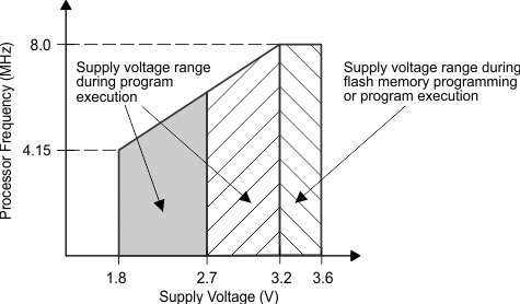
5.3 Recommended Operating Conditions
Typical values are specified at VCC = 3.3 V and TA = 25°C (unless otherwise noted)| MIN | NOM | MAX | UNIT | ||||
|---|---|---|---|---|---|---|---|
| VCC | Supply voltage (AVCC = DVCC = VCC) | During program execution | 1.8 | 3.6 | V | ||
| During flash memory programming | 2.7 | 3.6 | |||||
| VSS | Supply voltage (AVSS = DVSS = VSS) | 0 | 0 | V | |||
| TA | Operating free-air temperature | –40 | 85 | °C | |||
| fLFXT1 | LFXT1 crystal frequency(1) | LF selected, XTS = 0, watch crystal | 32768 | Hz | |||
| XT1 selected, XTS = 1, ceramic resonator | 450 | 8000 | kHz | ||||
| XT1 selected, XTS = 1, crystal | 1000 | 8000 | |||||
| fXT2 | XT2 crystal frequency(1) | Ceramic resonator | 450 | 8000 | kHz | ||
| Crystal | 1000 | 8000 | |||||
| fSYSTEM | Processor frequency (signal MCLK) | VCC = 1.8 V | DC | 4.15 | MHz | ||
| VCC = 3.6 V | DC | 8 | |||||
(1) In LF mode, the LFXT1 oscillator requires a watch crystal. TI recommends a 5.1-MΩ resistor from XOUT to VSS when VCC < 2.5 V.
In XT1 mode, the LFXT1 and XT2 oscillators accept a ceramic resonator or crystal up to 4.15 MHz at VCC ≥ 2.2 V.
In XT1 mode, the LFXT1 and XT2 oscillators accept a ceramic resonator or crystal up to 8 MHz at VCC ≥ 2.8 V.
In XT1 mode, the LFXT1 and XT2 oscillators accept a ceramic resonator or crystal up to 4.15 MHz at VCC ≥ 2.2 V.
In XT1 mode, the LFXT1 and XT2 oscillators accept a ceramic resonator or crystal up to 8 MHz at VCC ≥ 2.8 V.
 Figure 5-1 Frequency vs Supply Voltage