SLAS998A June 2014 – October 2018 MSP430F67621 , MSP430F67641
PRODUCTION DATA.
- 1Device Overview
- 2Revision History
- 3Device Comparison
- 4Terminal Configuration and Functions
-
5Specifications
- 5.1 Absolute Maximum Ratings
- 5.2 ESD Ratings
- 5.3 Recommended Operating Conditions
- 5.4 Active Mode Supply Current Into VCC Excluding External Current
- 5.5 Low-Power Mode Supply Currents (Into VCC) Excluding External Current
- 5.6 Low-Power Mode With LCD Supply Currents (Into VCC) Excluding External Current
- 5.7 Thermal Resistance Characteristics
- 5.8
Timing and Switching Characteristics
- 5.8.1 Clock Specifications
- 5.8.2
Digital I/O Ports
- Table 5-5 Schmitt-Trigger Inputs – General-Purpose I/O
- Table 5-6 Inputs – Ports P1 and P2
- Table 5-7 Leakage Current – General-Purpose I/O
- Table 5-8 Outputs – General-Purpose I/O (Full Drive Strength)
- Table 5-9 Typical Characteristics – General-Purpose I/O (Full Drive Strength)
- Table 5-10 Outputs – General-Purpose I/O (Reduced Drive Strength)
- 5.8.2.1 Typical Characteristics – General-Purpose I/O (Reduced Drive Strength)
- Table 5-11 Output Frequency – General-Purpose I/O
- 5.8.3 Power-Management Module (PMM)
- 5.8.4
Auxiliary Supplies
- Table 5-19 Auxiliary Supplies, Recommended Operating Conditions
- Table 5-20 Auxiliary Supplies, AUXVCC3 (Backup Subsystem) Currents
- Table 5-21 Auxiliary Supplies, Auxiliary Supply Monitor
- Table 5-22 Auxiliary Supplies, Switch ON-Resistance
- Table 5-23 Auxiliary Supplies, Switching Time
- Table 5-24 Auxiliary Supplies, Switch Leakage
- Table 5-25 Auxiliary Supplies, Auxiliary Supplies to ADC10_A
- Table 5-26 Auxiliary Supplies, Charge Limiting Resistor
- 5.8.5 Timer_A
- 5.8.6 eUSCI
- 5.8.7 LCD Controller
- 5.8.8
SD24_B
- Table 5-36 SD24_B Power Supply and Recommended Operating Conditions
- Table 5-37 SD24_B Analog Input
- Table 5-38 SD24_B Supply Currents
- Table 5-39 SD24_B Performance
- Table 5-40 SD24_B AC Performance
- Table 5-41 SD24_B AC Performance
- Table 5-42 SD24_B AC Performance
- Table 5-43 SD24_B External Reference Input
- 5.8.9 ADC10_A
- 5.8.10 REF
- 5.8.11 Flash Memory
- 5.8.12 Emulation and Debug
-
6Detailed Description
- 6.1 Overview
- 6.2 Functional Block Diagrams
- 6.3 CPU
- 6.4 Instruction Set
- 6.5 Operating Modes
- 6.6 Interrupt Vector Addresses
- 6.7 Memory Organization
- 6.8 Bootloader (BSL)
- 6.9 JTAG Operation
- 6.10 Flash Memory
- 6.11 RAM
- 6.12 Backup RAM
- 6.13
Peripherals
- 6.13.1 Oscillator and System Clock
- 6.13.2 Power Management Module (PMM)
- 6.13.3 Auxiliary Supply System (AUX)
- 6.13.4 Backup Subsystem
- 6.13.5 Digital I/O
- 6.13.6 Port Mapping Controller
- 6.13.7 System Module (SYS)
- 6.13.8 Watchdog Timer (WDT_A)
- 6.13.9 DMA Controller
- 6.13.10 CRC16
- 6.13.11 Hardware Multiplier
- 6.13.12 Enhanced Universal Serial Communication Interface (eUSCI)
- 6.13.13 ADC10_A
- 6.13.14 SD24_B
- 6.13.15 TA0
- 6.13.16 TA1
- 6.13.17 TA2
- 6.13.18 TA3
- 6.13.19 SD24_B Triggers
- 6.13.20 ADC10_A Triggers
- 6.13.21 Real-Time Clock (RTC_C)
- 6.13.22 Reference (REF) Module Voltage Reference
- 6.13.23 LCD_C
- 6.13.24 Embedded Emulation Module (EEM) (S Version)
- 6.13.25 Peripheral File Map
- 6.14
Input/Output Diagrams
- 6.14.1 Port P1 (P1.0 and P1.1) Input/Output With Schmitt Trigger
- 6.14.2 Port P1 (P1.2), Input/Output With Schmitt Trigger
- 6.14.3 Port P1 (P1.3 to P1.5) Input/Output With Schmitt Trigger
- 6.14.4 Port P1 (P1.6 and P1.7), Port P2 (P2.0 and P2.1) (PZ Package Only) Input/Output With Schmitt Trigger
- 6.14.5 Port P2 (P2.2 to P2.7) Input/Output With Schmitt Trigger (PZ Package Only)
- 6.14.6 Port P3 (P3.0 to P3.3) Input/Output With Schmitt Trigger (PZ Package Only)
- 6.14.7 Port P3 (P3.4 to P3.7) Input/Output With Schmitt Trigger (PZ Package Only)
- 6.14.8 Port P4 (P4.0 to P4.7), Port P5 (P5.0 to P5.7), Port P6 (P6.0 to P6.7), Port P7 (P7.0 to P7.7), Port P8 (P8.0 to P8.3) Input/Output With Schmitt Trigger (PZ Package Only)
- 6.14.9 Port P8 (P8.4 to P8.7) Input/Output With Schmitt Trigger (PZ Package Only)
- 6.14.10 Port P9 (P9.0) Input/Output With Schmitt Trigger (PZ Package Only)
- 6.14.11 Port P9 (P9.1 to P9.3) Input/Output With Schmitt Trigger (PZ Package Only)
- 6.14.12 Port P2 (P2.0 and P2.1) Input/Output With Schmitt Trigger (PN Package Only)
- 6.14.13 Port P2 (P2.2 to P2.7) Input/Output With Schmitt Trigger (PN Package Only)
- 6.14.14 Port P3 (P3.0 to P3.7) Input/Output With Schmitt Trigger (PN Package Only)
- 6.14.15 Port P4 (P4.0 to P4.7), Port P5 (P5.0 to P5.7), Port P6 (P6.0 to P6.7) Input/Output With Schmitt Trigger (PN Package Only)
- 6.14.16 Port PJ (PJ.0) JTAG Pin TDO, Input/Output With Schmitt Trigger or Output
- 6.14.17 Port PJ (PJ.1 to PJ.3) JTAG Pins TMS, TCK, TDI/TCLK, Input/Output With Schmitt Trigger or Output
- 6.15 Device Descriptors (TLV)
- 6.16 Identification
- 7Applications, Implementation, and Layout
- 8Device and Documentation Support
- 9Mechanical, Packaging, and Orderable Information
Package Options
Mechanical Data (Package|Pins)
Thermal pad, mechanical data (Package|Pins)
Orderable Information
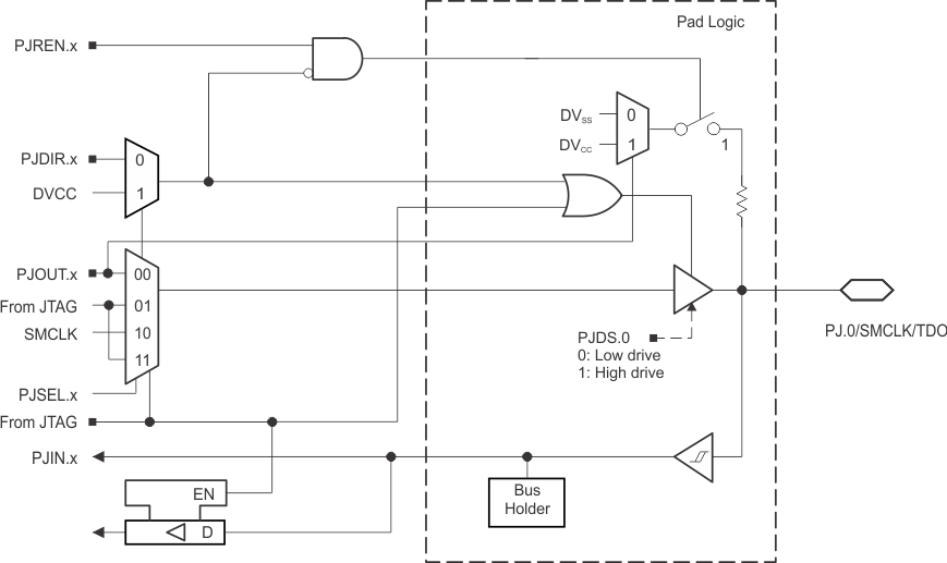
6.14.16 Port PJ (PJ.0) JTAG Pin TDO, Input/Output With Schmitt Trigger or Output
Figure 6-19 shows the port diagram. Table 6-79 summarizes the selection of the pin functions.
 Figure 6-19 Port PJ (PJ.0) Diagram