SLAS396D July 2003 – November 2016 MSP430FE423 , MSP430FE425 , MSP430FE427
PRODUCTION DATA.
- 1Device Overview
- 2Revision History
- 3Device Comparison
- 4Terminal Configuration and Functions
-
5Specifications
- 5.1 Absolute Maximum Ratings
- 5.2 ESD Ratings
- 5.3 Recommended Operating Conditions
- 5.4 Supply Current Into AVCC and DVCC Excluding External Current
- 5.5 Thermal Resistance Characteristics, PM Package (LQFP64)
- 5.6 Schmitt-Trigger Inputs − Ports (P1 and P2), RST/NMI, JTAG (TCK, TMS, TDI/TCLK,TDO/TDI)
- 5.7 Inputs P1.x, P2.x, TAx
- 5.8 Leakage Current − Ports (P1 and P2)
- 5.9 Outputs − Ports (P1 and P2)
- 5.10 Output Frequency
- 5.11 Typical Characteristics - Ports P1 and P2
- 5.12 Wake-up Time From LPM3
- 5.13 RAM
- 5.14 LCD
- 5.15 USART0
- 5.16 POR, BOR
- 5.17 SVS (Supply Voltage Supervisor and Monitor)
- 5.18 DCO
- 5.19 Crystal Oscillator, LFXT1 Oscillator
- 5.20 ESP430CE1, SD16 and ESP430 Power Supply and Operating Conditions
- 5.21 ESP430CE1, SD16 Input Range
- 5.22 ESP430CE1, SD16 Performance
- 5.23 ESP430CE1, SD16 Temperature Sensor
- 5.24 ESP430CE1, SD16 Built-in Voltage Reference
- 5.25 ESP430CE1, SD16 Reference Output Buffer
- 5.26 ESP430CE1, SD16 External Reference Input
- 5.27 ESP430CE1, Active Energy Measurement Test Conditions and Accuracy
- 5.28 ESP430CE1, Active Energy Measurement Test Conditions and Accuracy
- 5.29 ESP430CE1 Typical Characteristics (I1 SD16GAINx = 1)
- 5.30 ESP430CE1 Typical Characteristics (I1 SD16GAINx = 4)
- 5.31 ESP430CE1 Typical Characteristics (I1 SD16GAINx = 8)
- 5.32 ESP430CE1 Typical Characteristics (I1 SD16GAINx = 32)
- 5.33 Flash Memory
- 5.34 JTAG Interface
- 5.35 JTAG Fuse
-
6Detailed Description
- 6.1 CPU
- 6.2 Instruction Set
- 6.3 Operating Modes
- 6.4 Interrupt Vector Addresses
- 6.5 Special Function Registers
- 6.6 Memory Organization
- 6.7 Bootloader (BSL)
- 6.8 Flash Memory
- 6.9 Peripherals
- 6.10
Input/Output Diagrams
- 6.10.1 Port P1 (P1.0 and P1.1) Input/Output With Schmitt Trigger
- 6.10.2 Port P1 (P1.2 to P1.7) Input/Output With Schmitt Trigger
- 6.10.3 Port P2 (P2.0 and P2.1) Input/Output With Schmitt Trigger
- 6.10.4 Port P2 (P2.2 to P2.5) Input/Output With Schmitt Trigger
- 6.10.5 Port P2 (P2.6 and P2.7) Unbonded GPIOs
- 6.10.6 JTAG Pins TMS, TCK, TDI/TCLK, TDO/TDI, Input/Output With Schmitt-Trigger or Output
- 6.10.7 JTAG Fuse Check Mode
- 7Device and Documentation Support
- 8Mechanical, Packaging, and Orderable Information
Package Options
Mechanical Data (Package|Pins)
- PM|64
Thermal pad, mechanical data (Package|Pins)
Orderable Information
5 Specifications
5.1 Absolute Maximum Ratings(1)
over operating free-air temperature range (unless otherwise noted)| MIN | MAX | UNIT | |||
|---|---|---|---|---|---|
| Voltage applied at VCC to VSS | –0.3 | 4.1 | V | ||
| Voltage applied to any pin(2) | –0.3 | VCC + 0.3 | V | ||
| Diode current at any device terminal | ±2 | mA | |||
| Storage temperature range, Tstg | Unprogrammed device | –55 | 150 | °C | |
| Programmed device | –40 | 85 | |||
5.2 ESD Ratings
| VALUE | UNIT | |||
|---|---|---|---|---|
| V(ESD) | Electrostatic discharge | Human-body model (HBM), per ANSI/ESDA/JEDEC JS-001(1) | ±1000 | V |
| Charged-device model (CDM), per JEDEC specification JESD22-C101(2) | ±250 | |||
5.3 Recommended Operating Conditions
Typical values are specified at VCC = 3.3 V and TA = 25°C (unless otherwise noted)| MIN | NOM | MAX | UNIT | ||||
|---|---|---|---|---|---|---|---|
| VCC | Supply voltage during program execution(1) (AVCC = DVCC = VCC) | ESP430 and SD16 disabled | 1.8 | 3.6 | V | ||
| SVS enabled, PORON = 1(2), ESP430 and SD16 disabled | 2.0 | 3.6 | |||||
| ESP430 or SD16 enabled or during programming of flash memory | 2.7 | 3.6 | |||||
| VSS | Supply voltage (AVSS = DVSS = VSS) | 0 | 0 | V | |||
| TA | Operating free-air temperature range | –40 | 85 | °C | |||
| f(LFXT1) | LFXT1 crystal frequency(3) | LF selected, XTS_FLL = 0 | Watch crystal | 32.768 | kHz | ||
| XT1 selected, XTS_FLL = 1 | Ceramic resonator | 450 | 8000 | ||||
| XT1 selected, XTS_FLL = 1 | Crystal | 1000 | 8000 | ||||
| f(System) | Processor frequency (signal MCLK)(4) (also see Figure 5-1) | VCC = 2.7 V | DC | 8.4 | MHz | ||
| VCC = 3.6 V | DC | 8.4 | |||||
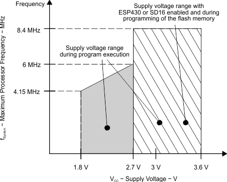 Figure 5-1 Frequency vs Supply Voltage
5.4 Supply Current Into AVCC and DVCC Excluding External Current(1)
over recommended operating free-air temperature range (unless otherwise noted)| PARAMETER | TA | VCC | MIN | TYP | MAX | UNIT | |
|---|---|---|---|---|---|---|---|
| I(AM) | Active mode (AM) f(MCLK) = f(SMCLK) = f(DCO) = 1 MHz, f(ACLK) = 32768 Hz, XTS_FLL = 0, program executes in flash |
–40°C to 85°C | 3 V | 400 | 500 | µA | |
| I(LPM0) | Low-power mode 0 or 1 (LPM0 or LPM1)(2)
f(MCLK) = f(SMCLK) = f(DCO) = 1 MHz, f(ACLK) = 32768 Hz, XTS_FLL = 0, FN_8 = FN_4 = FN_3 = FN_2 = 0 |
–40°C to 85°C | 3 V | 130 | 150 | µA | |
| I(LPM2) | Low-power mode 2 (LPM2)(2) | –40°C to 85°C | 3 V | 10 | 22 | µA | |
| I(LPM3) | Low-power mode 3 (LPM3) (2) | –40°C | 3 V | 1.5 | 2.0 | µA | |
| 25°C | 1.6 | 2.1 | |||||
| 60°C | 1.7 | 2.2 | |||||
| 85°C | 2.0 | 3.5 | |||||
| I(LPM4) | Low-power mode 4 (LPM4)(2) | –40°C | 3 V | 0.1 | 0.5 | µA | |
| 25°C | 0.1 | 0.5 | |||||
| 85°C | 0.8 | 2.5 | |||||
Current consumption of active mode versus system frequency:
I(AM) = I(AM) [1 MHz] × f(System) [MHz]
Current consumption of active mode versus supply voltage:
I(AM) = I(AM) [3 V] + 170 µA/V × (VCC – 3 V)
5.5 Thermal Resistance Characteristics, PM Package (LQFP64)
| PARAMETER | VALUE | UNIT | |
|---|---|---|---|
| RθJA | Junction-to-ambient thermal resistance, still air(1) | 55.7 | °C/W |
| RθJC(TOP) | Junction-to-case (top) thermal resistance(2) | 16.7 | °C/W |
| RθJB | Junction-to-board thermal resistance(3) | 27.1 | °C/W |
| ΨJB | Junction-to-board thermal characterization parameter | 26.8 | °C/W |
| ΨJT | Junction-to-top thermal characterization parameter | 0.8 | °C/W |
5.6 Schmitt-Trigger Inputs − Ports (P1 and P2), RST/NMI, JTAG (TCK, TMS, TDI/TCLK,TDO/TDI)
over recommended operating free-air temperature range (unless otherwise noted)| PARAMETER | VCC | MIN | MAX | UNIT | |
|---|---|---|---|---|---|
| VIT+ | Positive-going input threshold voltage | 3 V | 1.5 | 1.98 | V |
| VIT- | Negative-going input threshold voltage | 3 V | 0.9 | 1.3 | V |
| Vhys | Input voltage hysteresis (VIT+ - VIT- ) | 3 V | 0.45 | 1 | V |
5.7 Inputs P1.x, P2.x, TAx
over recommended operating free-air temperature range (unless otherwise noted)| PARAMETER | TEST CONDITIONS | VCC | MIN | MAX | UNIT | |
|---|---|---|---|---|---|---|
| t(int) | External interrupt timing | Port P1, P2: P1.x to P2.x, external trigger signal for the interrupt flag(1) | 3 V | 1.5 | cycle | |
| 50 | ns | |||||
| t(cap) | Timer_A capture timing | TAx | 3 V | 50 | ns | |
| f(TAext) | Timer_A clock frequency externally applied to pin | TAxCLK, INCLK t(H) = t(L) | 3 V | 10 | MHz | |
| f(TAint) | Timer_A clock frequency | SMCLK or ACLK signal selected | 3 V | 10 | MHz | |
5.8 Leakage Current − Ports (P1 and P2)(1)
over recommended operating free-air temperature range (unless otherwise noted)| PARAMETER | TEST CONDITIONS | VCC | MIN | MAX | UNIT | |
|---|---|---|---|---|---|---|
| Ilkg(P1.x) | Leakage current, Port P1.x | Port 1: V(P1.x) (2) | 3 V | ±50 | nA | |
| Ilkg(P2.x) | Leakage current, Port P2.x | Port 2: V(P2.x) (2) | 3 V | ±50 | nA | |
5.9 Outputs − Ports (P1 and P2)
over recommended operating free-air temperature range (unless otherwise noted)| PARAMETER | TEST CONDITIONS | VCC | MIN | MAX | UNIT | |
|---|---|---|---|---|---|---|
| VOH | High-level output voltage | IOH(max) = –1.5 mA(1) | 3 V | VCC – 0.25 | VCC | V |
| IOH(max) = –6 mA(2) | 3 V | VCC – 0.6 | VCC | |||
| VOL | Low-level output voltage | IOL(max) = 1.5 mA(1) | 3 V | VSS | VSS + 0.25 | V |
| IOL(max) = 6 mA(2) | 3 V | VSS | VSS + 0.6 | |||
5.10 Output Frequency
over recommended operating free-air temperature range (unless otherwise noted)| PARAMETER | TEST CONDITIONS | MIN | TYP | MAX | UNIT | ||
|---|---|---|---|---|---|---|---|
| f(Px.y) | Output frequency (1 ≤ × ≤ 2, 0 ≤ y ≤ 7) |
CL = 20 F, IL = ±1.5 mA, VCC = 3 V | DC | 12 | MHz | ||
| f(ACLK), | P1.1/TA0/MCLK, P1.5/TACLK/ACLK/S28 |
CL = 20 pF, VCC = 3 V | 12 | MHz | |||
| f(MCLK), | |||||||
| f(SMCLK) | |||||||
| t(Xdc) | Duty cycle of output frequency | P1.5/TACLK/ACLK/S28, CL = 20 pF, VCC = 3 V |
fACLK = fLFXT1 = fXT1 | 40% | 60% | ||
| fACLK = fLFXT1 = fLF | 30% | 70% | |||||
| fACLK = fLFXT1 | 50% | ||||||
| P1.1/TA0/MCLK, CL = 20 pF, VCC = 3 V, fMCLK = fDCOCLK |
50% – 15 ns | 50% | 50% + 15 ns | ||||
5.11 Typical Characteristics – Ports P1 and P2
Figure 5-2 through Figure 5-5 show the typical output currents of Ports P1 and P2. One output loaded at a time.
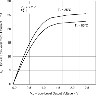 Figure 5-2 Typical Low-Level Output Current vs
 Low-Level Output Voltage
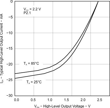 Figure 5-4 Typical High-Level Output Current vs
 High-Level Output Voltage
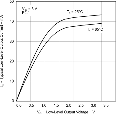 Figure 5-3 Typical Low-Level Output Current vs
 Low-Level Output Voltage
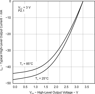 Figure 5-5 Typical High-Level Output Current vs
 High-Level Output Voltage
5.12 Wake-up Time From LPM3
over recommended operating free-air temperature range (unless otherwise noted)| PARAMETER | TEST CONDITIONS | MIN | MAX | UNIT | ||
|---|---|---|---|---|---|---|
| td(LPM3) | Delay time | f = 1 MHz | VCC = 3 V | 6 | µs | |
| f = 2 MHz | 6 | |||||
| f = 3 MHz | 6 | |||||
5.13 RAM
over recommended operating free-air temperature range (unless otherwise noted)| PARAMETER | TEST CONDITIONS | MIN | MAX | UNIT | ||
|---|---|---|---|---|---|---|
| VRAMh | CPU halted(1) | 1.6 | V | |||
5.14 LCD
over recommended operating free-air temperature range (unless otherwise noted)| PARAMETER | TEST CONDITIONS | MIN | TYP | MAX | UNIT | ||
|---|---|---|---|---|---|---|---|
| V(33) | Analog voltage | Voltage at R33 | VCC = 3 V | 2.5 | VCC + 0.2 | V | |
| V(23) | Voltage at R23 | [V(33) – V(03)] × 2/3 + V(03) | |||||
| V(13) | Voltage at R13 | [V(33) – V(03)] × 1/3 + V(03) | |||||
| V(33) – V(03) | Voltage at R33 to R03 | 2.5 | VCC + 0.2 | ||||
| I(R03) | Input leakage | R03 = VSS | No load at all segment and common lines, VCC = 3 V |
±20 | nA | ||
| I(R13) | R13 = VCC / 3 | ±20 | |||||
| I(R23) | R23 = 2 × VCC / 3 | ±20 | |||||
| V(Sxx0) | Segment line voltage | I(Sxx) = –3 µA, VCC = 3 V | V(03) | V(03) – 0.1 | V | ||
| V(Sxx1) | V(13) | V(13) – 0.1 | |||||
| V(Sxx2) | V(23) | V(23) – 0.1 | |||||
| V(Sxx3) | V(33) | V(33) + 0.1 | |||||
5.15 USART0(1)
over recommended operating free-air temperature range (unless otherwise noted)| PARAMETER | TEST CONDITIONS | MIN | TYP | MAX | UNIT | |
|---|---|---|---|---|---|---|
| t(τ) | USART0 deglitch time | VCC = 3 V, SYNC = 0, UART mode | 150 | 280 | 500 | ns |
5.16 POR, BOR(1)
over recommended operating free-air temperature range (unless otherwise noted)| PARAMETER | TEST CONDITIONS | MIN | TYP | MAX | UNIT | |
|---|---|---|---|---|---|---|
| td(BOR) | Brownout(2) | 2000 | µs | |||
| VCC(start) | dVCC/dt ≤ 3 V/s (see Figure 5-6) | 0.7 × V(B_IT– ) | V | |||
| V(B_IT–) | dVCC/dt ≤ 3 V/s (see Figure 5-6 through Figure 5-8) | 1.71 | V | |||
| Vhys(B_IT–) | dVCC/dt ≤ 3 V/s (see Figure 5-6) | 70 | 130 | 180 | mV | |
| t(reset) | Pulse duration needed at RST/NMI pin to accept reset internally, VCC = 3 V | 2 | µs | |||
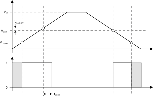 Figure 5-6 POR and BOR vs Supply Voltage
 Figure 5-7 VCC(drop) Level With a Rectangular Voltage Drop to Generate a POR/Brownout Signal
 Figure 5-8 VCC(drop) Level With a Triangular Voltage Drop to Generate a POR or BOR Signal
5.17 SVS (Supply Voltage Supervisor and Monitor)(3)
over recommended operating free-air temperature range (unless otherwise noted) (also see Figure 5-10)| PARAMETER | TEST CONDITIONS | MIN | TYP | MAX | UNIT | |
|---|---|---|---|---|---|---|
| t(SVSR) | dVCC/dt > 30 V/ms (see Figure 5-9) | 5 | 150 | µs | ||
| dVCC/dt ≤ 30 V/ms | 2000 | |||||
| td(SVSon) | SVS on, switch from VLD = 0 to VLD ≠ 0, VCC = 3 V | 20 | 150 | µs | ||
| tsettle | VLD ≠ 0(2) | 12 | µs | |||
| V(SVSstart) | VLD ≠ 0, VCC/dt ≤ 3 V/s (see Figure 5-9) | 1.55 | 1.7 | V | ||
| Vhys(SVS_IT–) | VCC/dt ≤ 3 V/s (see Figure 5-9) | VLD = 1 | 70 | 120 | 155 | mV |
| VLD = 2 to 14 | V(SVS_IT–) × 0.004 | V(SVS_IT–) × 0.008 | ||||
| VCC/dt ≤ 3 V/s (see Figure 5-9), external voltage applied on P2.3 | VLD = 15 | 4.4 | 10.4 | mV | ||
| V(SVS_IT–) | VCC/dt ≤ 3 V/s (see Figure 5-9) | VLD = 1 | 1.8 | 1.9 | 2.05 | V |
| VLD = 2 | 1.94 | 2.1 | 2.25 | |||
| VLD = 3 | 2.05 | 2.2 | 2.37 | |||
| VLD = 4 | 2.14 | 2.3 | 2.48 | |||
| VLD = 5 | 2.24 | 2.4 | 2.6 | |||
| VLD = 6 | 2.33 | 2.5 | 2.71 | |||
| VLD = 7 | 2.46 | 2.65 | 2.86 | |||
| VLD = 8 | 2.58 | 2.8 | 3 | |||
| VLD = 9 | 2.69 | 2.9 | 3.13 | |||
| VLD = 10 | 2.83 | 3.05 | 3.29 | |||
| VLD = 11 | 2.94 | 3.2 | 3.42 | |||
| VLD = 12 | 3.11 | 3.35 | 3.61(1) | |||
| VLD = 13 | 3.24 | 3.5 | 3.76(1) | |||
| VLD = 14 | 3.43 | 3.7(1) | 3.99(1) | |||
| VCC/dt ≤ 3 V/s (see Figure 5-9), external voltage applied on P2.3 | VLD = 15 | 1.1 | 1.2 | 1.3 | ||
| ICC(SVS)(3) | VLD ≠ 0, VCC = 2.2 V or 3 V | 10 | 15 | µA | ||
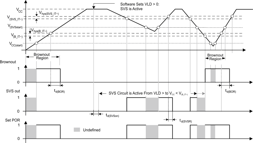 Figure 5-9 SVS Reset (SVSR) vs Supply Voltage
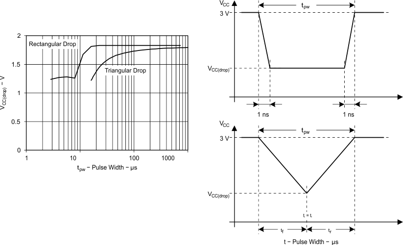 Figure 5-10 VCC(drop) With a Rectangular Voltage Drop and a Triangular Voltage Drop to Generate an SVS Signal
5.18 DCO
over recommended operating free-air temperature range (unless otherwise noted) (also see Figure 5-11 through Figure 5-13)| PARAMETER | TEST CONDITIONS | VCC | MIN | TYP | MAX | UNIT |
|---|---|---|---|---|---|---|
| f(DCOCLK) | N(DCO) = 01Eh, FN_8 = FN_4 = FN_3 = FN_2 = 0, D = 2, DCOPLUS = 0, fCrystal = 32.768 kHz | 3 V | 1 | MHz | ||
| f(DCO = 2) | FN_8 = FN_4 = FN_3 = FN_2 = 0, DCOPLUS = 1 | 3 V | 0.3 | 0.7 | 1.3 | MHz |
| f(DCO = 27) | FN_8 = FN_4 = FN_3 = FN_2 = 0, DCOPLUS = 1 | 3 V | 2.7 | 6.1 | 11.3 | MHz |
| f(DCO = 2) | FN_8 = FN_4 = FN_3 = FN_2 = 1, DCOPLUS = 1 | 3 V | 0.8 | 1.5 | 2.5 | MHz |
| f(DCO = 27) | FN_8 = FN_4 = FN_3 = FN_2 = 1, DCOPLUS = 1 | 3 V | 6.5 | 12.1 | 20 | MHz |
| f(DCO = 2) | FN_8 = FN_4 = 0, FN_3 = 1, FN_2 = x, DCOPLUS = 1 | 3 V | 1.3 | 2.2 | 3.5 | MHz |
| f(DCO = 27) | FN_8 = FN_4 = 0, FN_3 = 1, FN_2 = x, DCOPLUS = 1 | 3 V | 10.3 | 17.9 | 28.5 | MHz |
| f(DCO = 2) | FN_8 = 0, FN_4 = 1, FN_3 = FN_2 = x, DCOPLUS = 1 | 3 V | 2.1 | 3.4 | 5.2 | MHz |
| f(DCO = 27) | FN_8 = 0, FN_4 = 1, FN_3 = FN_2 = x, DCOPLUS = 1 | 3 V | 16 | 26.6 | 41 | MHz |
| f(DCO = 2) | FN_8 = 1, FN_4 = 1 = FN_3 = FN_2 = x, DCOPLUS = 1 | 3 V | 4.2 | 6.3 | 9.2 | MHz |
| f(DCO = 27) | FN_8 = 1, FN_4 = 1 = FN_3 = FN_2 = x, DCOPLUS = 1 | 3 V | 30 | 46 | 70 | MHz |
| Sn | Step size (ratio) between adjacent DCO taps: Sn = fDCO(Tap n+1)/fDCO(Tap n) (see Figure 5-12 for taps 21 to 27) |
1 < TAP ≤ 20 | 1.06 | 1.11 | ||
| TAP = 27 | 1.07 | 1.17 | ||||
| Dt | Temperature drift, N(DCO) = 01Eh, FN_8 = FN_4 = FN_3 = FN_2 = 0, D = 2, DCOPLUS = 0 | 3 V | –0.2 | –0.3 | –0.4 | %/°C |
| DV | Drift with VCC variation, N(DCO) = 01Eh, FN_8 = FN_4 = FN_3 = FN_2 = 0, D = 2, DCOPLUS = 0 | 0 | 5 | 15 | %/V |
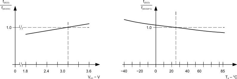 Figure 5-11 DCO Frequency vs Supply Voltage VCC and vs Ambient Temperature
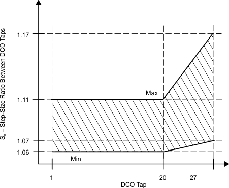 Figure 5-12 DCO Tap Step Size
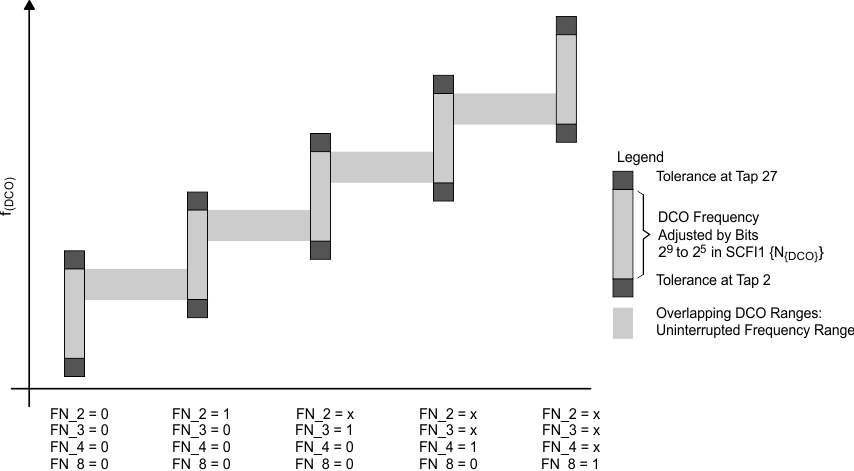 Figure 5-13 Five Overlapping DCO Ranges Controlled by FN_x Bits
5.19 Crystal Oscillator, LFXT1 Oscillator(1) (2)
over recommended operating free-air temperature range (unless otherwise noted)| PARAMETER | TEST CONDITIONS | VCC | MIN | TYP | MAX | UNIT | |
|---|---|---|---|---|---|---|---|
| CXIN | Integrated input capacitance(4) | OSCCAPx = 0h | 3 V | 0 | pF | ||
| OSCCAPx = 1h | 10 | ||||||
| OSCCAPx = 2h | 14 | ||||||
| OSCCAPx = 3h | 18 | ||||||
| CXOUT | Integrated output capacitance(4) | OSCCAPx = 0h | 3 V | 0 | pF | ||
| OSCCAPx = 1h | 10 | ||||||
| OSCCAPx = 2h | 14 | ||||||
| OSCCAPx = 3h | 18 | ||||||
| VIL | Input levels at XIN(3) | 2.2 V, 3 V | VSS | 0.2 × VCC | V | ||
| VIH | 0.8 × VCC | VCC | |||||
- Keep the trace between the device and the crystal as short as possible.
- Design a good ground plane around the oscillator pins.
- Prevent crosstalk from other clock or data lines into oscillator pins XIN and XOUT.
- Avoid running PCB traces underneath or adjacent to the XIN and XOUT pins.
- Use assembly materials and processes that avoid any parasitic load on the oscillator XIN and XOUT pins.
- If conformal coating is used, ensure that it does not induce capacitive or resistive leakage between the oscillator pins.
- Do not route the XOUT line to the JTAG header to support the serial programming adapter as shown in other documentation. This signal is no longer required for the serial programming adapter.
5.20 ESP430CE1, SD16 and ESP430 Power Supply and Operating Conditions
over recommended operating free-air temperature range (unless otherwise noted)| PARAMETER | TEST CONDITIONS | VCC | MIN | TYP | MAX | UNIT | ||
|---|---|---|---|---|---|---|---|---|
| AVCC | Analog supply voltage | AVCC = DVCC, AVSS = DVSS = 0 V | 2.7 | 3.6 | V | |||
| IESP430CE1 | Total digital and analog supply current when ESP430 and SD16 active (IAVCC + IDVCC) | SD16LP = 0, fMCLK = 4 MHz, fSD16 = fMCLK / 4, SD16REFON = 1, SD16VMIDON = 0 |
GAIN(V): 1, GAIN(I1): 1, I2: off | 3 V | 2.0 | 2.6 | mA | |
| GAIN(V): 1, GAIN(I1): 32, I2: off | 2.4 | 3.3 | ||||||
| GAIN(V): 1, GAIN(I1): 1, GAIN(I2): 1 | 2.7 | 3.6 | ||||||
| GAIN(V): 1, GAIN(I1): 32, GAIN(I2): 32 | 3.4 | 4.9 | ||||||
| SD16LP = 1, fMCLK = 2 MHz, fSD16 = fMCLK / 4, SD16REFON = 1, SD16VMIDON = 0 |
GAIN(V): 1, GAIN(I1): 1, I2: off | 1.5 | 2.1 | |||||
| GAIN(V): 1, GAIN(I1): 32, I2: off | 1.6 | 2.1 | ||||||
| GAIN(V): 1, GAIN(I1): 1, GAIN(I2): 1 | 2.1 | 2.8 | ||||||
| GAIN(V): 1, GAIN(I1): 32, GAIN(I2): 32 | 2.2 | 3.0 | ||||||
| ISD16 | Analog supply current: 1 active SD16 channel including internal reference (ESP430 disabled) | SD16LP = 0, fSD16 = 1 MHz, SD16OSR = 256 |
GAIN: 1, 2 | 3 V | 650 | 950 | µA | |
| GAIN: 4, 8, 16 | 730 | 1100 | ||||||
| GAIN: 32 | 1050 | 1550 | ||||||
| SD16LP = 1, fSD16 = 0.5 MHz, SD16OSR = 256 |
GAIN: 1 | 620 | 930 | |||||
| GAIN: 32 | 700 | 1060 | ||||||
| fMAINS | Mains frequency range | 33 | 80 | Hz | ||||
| fSD16 | Analog front-end input clock frequency | SD16LP = 0 (low-power mode disabled) | 1 | MHz | ||||
| SD16LP = 1 (low-power mode enabled) | 0.5 | |||||||
5.21 ESP430CE1, SD16 Input Range(1)
over operating free-air temperature range (unless otherwise noted)| PARAMETER | TEST CONDITIONS | VCC | MIN | TYP | MAX | UNIT | |
|---|---|---|---|---|---|---|---|
| VID | Differential input voltage range for specified performance(2) | SD16GAINx = 1, SD16REFON = 1 | ±500 | mV | |||
| SD16GAINx = 2, SD16REFON = 1 | ±250 | ||||||
| SD16GAINx = 4, SD16REFON = 1 | ±125 | ||||||
| SD16GAINx = 8, SD16REFON = 1 | ±62 | ||||||
| SD16GAINx = 16, SD16REFON = 1 | ±31 | ||||||
| SD16GAINx = 32, SD16REFON = 1 | ±15 | ||||||
| ZI | Input impedance (one input pin to AVSS) |
fSD16 = 1 MHz, SD16GAINx = 1 | 3 V | 200 | kΩ | ||
| fSD16 = 1 MHz, SD16GAINx = 32 | 75 | ||||||
| ZID | Differential input impedance (IN+ to IN−) |
fSD16 = 1 MHz, SD16GAINx = 1 | 3 V | 300 | 400 | kΩ | |
| fSD16 = 1 MHz, SD16GAINx = 32 | 100 | 150 | |||||
| VI | Absolute input voltage range | AVSS – 1 | AVCC | V | |||
| VIC | Common-mode input voltage range | AVSS – 1 | AVCC | V | |||
5.22 ESP430CE1, SD16 Performance
fSD16 = 1 MHz, SD16OSRx = 256, SD16REFON = 1, over operating free-air temperature range (unless otherwise noted)| PARAMETER | TEST CONDITIONS | VCC | MIN | TYP | MAX | UNIT | ||
|---|---|---|---|---|---|---|---|---|
| SINAD | Signal-to-noise + distortion ratio | SD16GAINx = 1, signal amplitude = 500 mV | fIN = 50 Hz or 100 Hz | 3 V | 83.5 | 85 | dB | |
| SD16GAINx = 2, signal amplitude = 250 mV | 81.5 | 84 | ||||||
| SD16GAINx = 4, signal amplitude = 125 mV | 76 | 79.5 | ||||||
| SD16GAINx = 8, signal amplitude = 62 mV | 73 | 76.5 | ||||||
| SD16GAINx = 16, signal amplitude = 31 mV | 69 | 73 | ||||||
| SD16GAINx = 32, signal amplitude = 15 mV | 62 | 69 | ||||||
| G | Nominal gain | SD16GAINx = 1 | 3 V | 0.97 | 1.00 | 1.02 | ||
| SD16GAINx = 2 | 1.90 | 1.96 | 2.02 | |||||
| SD16GAINx = 4 | 3.76 | 3.86 | 3.96 | |||||
| SD16GAINx = 8 | 7.36 | 7.62 | 7.84 | |||||
| SD16GAINx = 16 | 14.56 | 15.04 | 15.52 | |||||
| SD16GAINx = 32 | 27.20 | 28.35 | 29.76 | |||||
| EOS | Offset error | SD16GAINx = 1 | 3 V | ±0.2 | %FSR | |||
| SD16GAINx = 32 | ±1.5 | |||||||
| dEOS/dT | Offset error temperature coefficient | SD16GAINx = 1 | 3 V | ±4 | ±20 | ppm FSR/°C | ||
| SD16GAINx = 32 | ±20 | ±100 | ||||||
| CMRR | Common-mode rejection ratio | SD16GAINx = 1, Common-mode input signal: VID = 500 mV, fIN = 50 Hz or 100 Hz |
3 V | >90 | dB | |||
| SD16GAINx = 32, Common-mode input signal: VID = 16 mV, fIN = 50 Hz or 100 Hz |
>75 | |||||||
| AC PSRR | AC power-supply rejection ratio | SD16GAINx = 1, VCC = 3 V ±100 mV, fVCC = 50 Hz | 3 V | >80 | dB | |||
| XT | Crosstalk | 3 V | <–100 | dB | ||||
5.23 ESP430CE1, SD16 Temperature Sensor(1)
over operating free-air temperature range (unless otherwise noted)| PARAMETER | TEST CONDITIONS | VCC | MIN | TYP | MAX | UNIT | |
|---|---|---|---|---|---|---|---|
| TCSensor | Sensor temperature coefficient | 1.18 | 1.32 | 1.46 | mV/K | ||
| VOffset,sensor | Sensor offset voltage | –100 | 100 | mV | |||
| VSensor | Sensor output voltage(2) | Temperature sensor voltage at TA = 85°C | 3 V | 435 | 475 | 515 | mV |
| Temperature sensor voltage at TA = 25°C | 355 | 395 | 435 | ||||
| Temperature sensor voltage at TA = 0°C | 320 | 360 | 400 | ||||
VSensor,typ = TCSensor (273 + T [°C] ) + VOffset,sensor [mV]
5.24 ESP430CE1, SD16 Built-in Voltage Reference
over operating free-air temperature range (unless otherwise noted)| PARAMETER | TEST CONDITIONS | VCC | MIN | TYP | MAX | UNIT | |
|---|---|---|---|---|---|---|---|
| VREF | Internal reference voltage | SD16REFON = 1, SD16VMIDON = 0 | 3 V | 1.14 | 1.20 | 1.26 | V |
| IREF | Reference supply current | SD16REFON = 1, SD16VMIDON = 0 | 3 V | 175 | 260 | µA | |
| TC | Temperature coefficient | SD16REFON = 1, SD16VMIDON = 0(1) | 3 V | 20 | 50 | ppm/K | |
| CREF | VREF load capacitance | SD16REFON = 1 SD16VMIDON = 0(2) | 100 | nF | |||
| ILOAD | VREF(I) maximum load current | SD16REFON = 0, SD16VMIDON = 0 | 3 V | ±200 | nA | ||
| tON | Turnon time | SD16REFON = 0 → 1, SD16VMIDON = 0, CREF = 100 nF |
3 V | 5 | ms | ||
| DC PSR | DC power supply rejection, ΔVREF/ΔVCC | SD16REFON = 1, SD16VMIDON = 0, VCC = 2.5 V to 3.6 V |
200 | µV/V | |||
5.25 ESP430CE1, SD16 Reference Output Buffer
over operating free-air temperature range (unless otherwise noted)| PARAMETER | TEST CONDITIONS | VCC | MIN | TYP | MAX | UNIT | |
|---|---|---|---|---|---|---|---|
| VREF,BUF | Reference buffer output voltage | SD16REFON = 1, SD16VMIDON = 1 | 3 V | 1.2 | V | ||
| IREF,BUF | Reference supply and reference output buffer quiescent current | SD16REFON = 1, SD16VMIDON = 1 | 3 V | 385 | 600 | A | |
| CREF(O) | Required load capacitance on VREF | SD16REFON = 1, SD16VMIDON = 1 | 470 | nF | |||
| ILOAD,Max | Maximum load current on VREF | SD16REFON = 1, SD16VMIDON = 1 | 3 V | ±1 | mA | ||
| Maximum voltage variation versus load current | |ILOAD| = 0 to 1 mA | 3 V | –15 | +15 | mV | ||
| tON | Turnon time | SD16REFON = 0 → 1, SD16VMIDON = 0, CREF = 100 nF |
3 V | 100 | µs | ||
5.26 ESP430CE1, SD16 External Reference Input
over operating free-air temperature range (unless otherwise noted)| PARAMETER | TEST CONDITIONS | VCC | MIN | TYP | MAX | UNIT | |
|---|---|---|---|---|---|---|---|
| VREF(I) | Input voltage | SD16REFON = 0 | 3 V | 1.0 | 1.25 | 1.5 | V |
| IREF(I) | Input current | SD16REFON = 0 | 3 V | 50 | nA | ||
5.27 ESP430CE1, Active Energy Measurement Test Conditions and Accuracy(1)
TA = 25°C, input conditions (unless otherwise noted): IB = 6 A, IMAX = n × IB = 60 A, n = 10, VN = 230 V, fMAINS = 50 Hz| PARAMETER | TEST CONDITIONS | VCC | TYP | UNIT | |
|---|---|---|---|---|---|
| Maximum error(2)(3) | I = 0.05 × IB, V = VN, PF = 1.0 | V1 SD16GAINx = 1, I1 SD16GAINx = 1, See Figure 5-14, R1 = 0 Ω, RB = 12.4 Ω |
3 V | ±0.17% | |
| I = 0.1 × IB to IMAX, V = VN, PF = 1.0 | ±0.18% | ||||
| I = 0.1 × IB, V = VN, PF = 0.5 lagging | ±0.19% | ||||
| I = 0.2 × IB to IMAX, V = VN, PF = 0.5 lagging | ±0.27% | ||||
| I = 0.1 × IB, V = VN, PF = 0.8 leading | ±0.15% | ||||
| I = 0.2 × IB to IMAX, V = VN, PF = 0.8 leading | ±0.24% | ||||
| I = 0.2 × IB to IMAX, V = VN, PF = 0.25 lagging | ±0.38% | ||||
- fACLK = 32768 Hz (watch crystal)
- fMCLK = 4.194 MHz (FLL+)
- fSD16 = fMCLK / 4 = 1.049 MHz
- Single-point calibration at I = 10 A and PF = 0.5 lagging
- Measurements according to IEC1036
I1 SD16GAINx = 8: shunt part number = A−H2−R005−F1−K2−0.1 (Isabellenhütte Heusler GmbH KG)
I1 SD16GAINx = 32: shunt part number = BVO−M−R0002−5.0 (Isabellenhütte Heusler GmbH KG)
5.28 ESP430CE1, Active Energy Measurement Test Conditions and Accuracy(1)
TA = 25°C, input conditions (unless otherwise noted): IB = 10 A, IMAX = n × IB = 60 A, n = 6, VN = 230 V, fMAINS = 50 Hz| PARAMETER | TEST CONDITIONS | VCC | TYP | UNIT | |
|---|---|---|---|---|---|
| Maximum error(2)(3) | I = 0.05 × IB, V = VN, PF = 1.0 | V1 SD16GAINx = 1, I1 SD16GAINx = 32, See Figure 5-15, Rshunt = 0.2 mΩ |
3 V | ±0.11% | |
| I = 0.1 × IB to IMAX, V = VN, PF = 1.0 | ±0.18% | ||||
| I = 0.1 × IB, V = VN, PF = 0.5 lagging | ±0.45% | ||||
| I = 0.2 × IB to IMAX, V = VN, PF = 0.5 lagging | ±0.33% | ||||
| I = 0.1 × IB, V = VN, PF = 0.8 leading | ±0.10% | ||||
| I = 0.2 × IB to IMAX, V = VN, PF = 0.8 leading | ±0.18% | ||||
| I = 0.2 × IB to IMAX, V = VN, PF = 0.25 lagging | ±0.51% | ||||
- fACLK = 32768 Hz (watch crystal)
- fMCLK = 4.194 MHz (FLL+)
- fSD16 = fMCLK / 4 = 1.049 MHz
- Single-point calibration at I = 10 A and PF = 0.5 lagging
- Measurements according to IEC1036
I1 SD16GAINx = 8: shunt part number = A−H2−R005−F1−K2−0.1 (Isabellenhütte Heusler GmbH KG)
I1 SD16GAINx = 32: shunt part number = BVO−M−R0002−5.0 (Isabellenhütte Heusler GmbH KG)
 Figure 5-14 Energy Measurement Test Circuitry (SD16GAINx = 1 or 4)
 Figure 5-15 Energy Measurement Test Circuitry (SD16GAINx = 8 or 32)
5.29 ESP430CE1 Typical Characteristics (I1 SD16GAINx = 1)
Results corrected for typical phase error of CT used (−40°C to 25°C: −0.7°; 25°C to 85°C: +0.5°). See Figure 5-14 for test circuitry: CT part number = T60404-E4624-X101 (Vacuumschmelze), R1 = 0 Ω, RB = 12.4 Ω
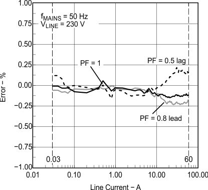 Figure 5-16 Measurement Error as Percentage of Reading (TA = 25°C)
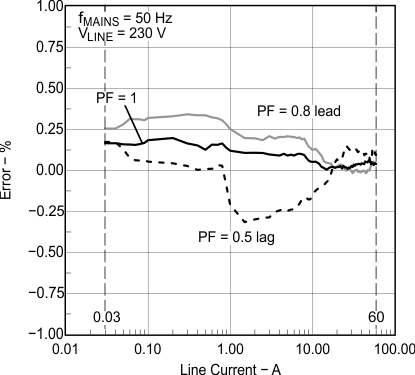 Figure 5-18 Measurement Error as Percentage of Reading (TA = 85°C)
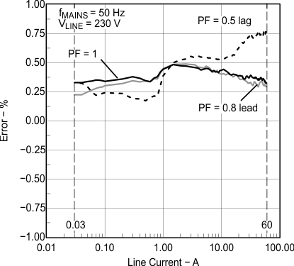 Figure 5-17 Measurement Error as Percentage of Reading (TA = –40°C)
5.30 ESP430CE1 Typical Characteristics (I1 SD16GAINx = 4)
Results corrected for typical phase error of CT used (−40°C to 25°C: −0.7°; 25°C to 85°C: +0.5°). See Figure 5-14 for test circuitry: CT part number = T60404-E4624-X101 (Vacuumschmelze), R1 = 9.36 Ω, RB = 3.16 Ω
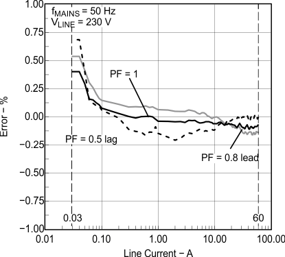 Figure 5-19 Measurement Error as Percentage of Reading (TA = 25°C)
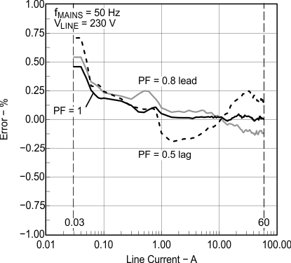 Figure 5-21 Measurement Error as Percentage of Reading (TA = 85°C)
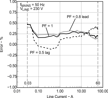 Figure 5-20 Measurement Error as Percentage of Reading (TA = –40°C)
5.31 ESP430CE1 Typical Characteristics (I1 SD16GAINx = 8)
See Figure 5-15 for test circuitry: shunt part number = A-H2-R005-F1-K2-0.1 (Isabellenhütte Heusler GmbH KG)
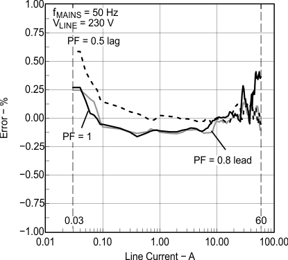 Figure 5-22 Measurement Error as Percentage of Reading (TA = 25°C)
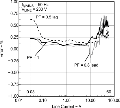 Figure 5-24 Measurement Error as Percentage of Reading (TA = 85°C)
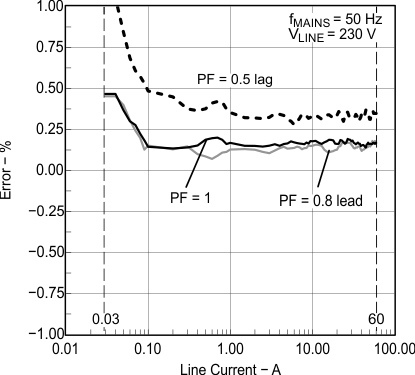 Figure 5-23 Measurement Error as Percentage of Reading (TA = –40°C)
5.32 ESP430CE1 Typical Characteristics (I1 SD16GAINx = 32)
See Figure 5-15 for test circuitry: shunt part number = BVO-M-R0002-5.0 (Isabellenhütte Heusler GmbH KG)
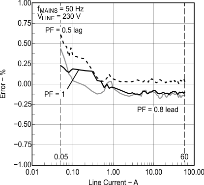 Figure 5-25 Measurement Error as Percentage of Reading (TA = 25°C)
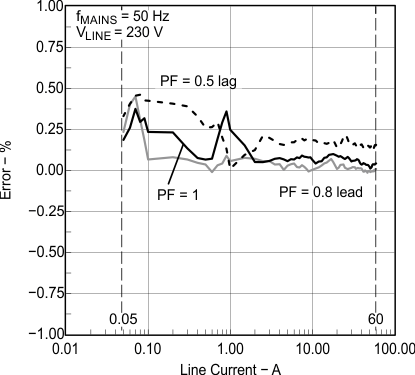 Figure 5-27 Measurement Error as Percentage of Reading (TA = 85°C)
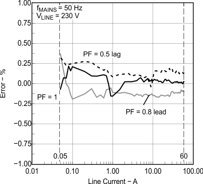 Figure 5-26 Measurement Error as Percentage of Reading (TA = –40°C)
5.33 Flash Memory
over recommended operating free-air temperature range (unless otherwise noted)| PARAMETER | TEST CONDITIONS | VCC | MIN | TYP | MAX | UNIT | |
|---|---|---|---|---|---|---|---|
| VCC(PGM/ ERASE) | Program and erase supply voltage | 2.7 | 3.6 | V | |||
| fFTG | Flash timing generator frequency | 257 | 476 | kHz | |||
| IPGM | Supply current from DVCC during program | 2.7 V, 3.6 V | 3 | 5 | mA | ||
| IERASE | Supply current from DVCC during erase | 2.7 V, 3.6 V | 3 | 7 | mA | ||
| tCPT | Cumulative program time | See (1) | 2.7 V, 3.6 V | 10 | ms | ||
| tCMErase | Cumulative mass erase time | See (2) | 2.7 V, 3.6 V | 200 | ms | ||
| Program and erase endurance | 104 | 105 | cycles | ||||
| tRetention | Data retention duration | TJ = 25°C | 100 | years | |||
| tWord | Word or byte program time | See (3) | 35 | tFTG | |||
| tBlock, 0 | Block program time for first byte or word | 30 | |||||
| tBlock, 1–63 | Block program time for each additional byte or word | 21 | |||||
| tBlock, End | Block program end-sequence wait time | 6 | |||||
| tMass Erase | Mass erase time | 5297 | |||||
| tSeg Erase | Segment erase time | 4819 | |||||
5.34 JTAG Interface
over recommended operating free-air temperature range (unless otherwise noted)| PARAMETER | TEST CONDITIONS | VCC | MIN | TYP | MAX | UNIT | |
|---|---|---|---|---|---|---|---|
| fTCK | TCK input frequency | See (1) | 2.2 V | 0 | 5 | MHz | |
| 3V | 0 | 10 | |||||
| RInternal | Internal pullup resistance on TMS, TCK, TDI/TCLK | See (2) | 2.2 V, 3 V | 25 | 60 | 90 | kΩ |
5.35 JTAG Fuse(1)
over recommended operating free-air temperature range (unless otherwise noted)| PARAMETER | TEST CONDITIONS | MIN | MAX | UNIT | |
|---|---|---|---|---|---|
| VCC(FB) | Supply voltage during fuse-blow condition | TA = 25°C | 2.5 | V | |
| VFB | Voltage level on TDI/TCLK for fuse-blow | 6 | 7 | V | |
| IFB | Supply current into TDI/TCLK during fuse blow | 100 | mA | ||
| tFB | Time to blow fuse | 1 | ms | ||