SLASEE4C January 2018 – December 2019 MSP430FR2512 , MSP430FR2522
PRODUCTION DATA.
- 1Device Overview
- 2Revision History
- 3Device Comparison
- 4Terminal Configuration and Functions
-
5Specifications
- 5.1 Absolute Maximum Ratings
- 5.2 ESD Ratings
- 5.3 Recommended Operating Conditions
- 5.4 Active Mode Supply Current Into VCC Excluding External Current
- 5.5 Active Mode Supply Current Per MHz
- 5.6 Low-Power Mode (LPM0) Supply Currents Into VCC Excluding External Current
- 5.7 Low-Power Mode (LPM3, LPM4) Supply Currents (Into VCC) Excluding External Current
- 5.8 Low-Power Mode (LPMx.5) Supply Currents (Into VCC) Excluding External Current
- 5.9 Typical Characteristics - Low-Power Mode Supply Currents
- Table 5-1 Typical Characteristics – Current Consumption Per Module
- 5.10 Thermal Resistance Characteristics
- 5.11 Timing and Switching Characteristics
-
6Detailed Description
- 6.1 Overview
- 6.2 CPU
- 6.3 Operating Modes
- 6.4 Interrupt Vector Addresses
- 6.5 Bootloader (BSL)
- 6.6 JTAG Standard Interface
- 6.7 Spy-Bi-Wire Interface (SBW)
- 6.8 FRAM
- 6.9 Memory Protection
- 6.10
Peripherals
- 6.10.1 Power-Management Module (PMM)
- 6.10.2 Clock System (CS) and Clock Distribution
- 6.10.3 General-Purpose Input/Output Port (I/O)
- 6.10.4 Watchdog Timer (WDT)
- 6.10.5 System (SYS) Module
- 6.10.6 Cyclic Redundancy Check (CRC)
- 6.10.7 Enhanced Universal Serial Communication Interface (eUSCI_A0, eUSCI_B0)
- 6.10.8 Timers (Timer0_A3, Timer1_A3)
- 6.10.9 Hardware Multiplier (MPY)
- 6.10.10 Backup Memory (BAKMEM)
- 6.10.11 Real-Time Clock (RTC)
- 6.10.12 10-Bit Analog-to-Digital Converter (ADC)
- 6.10.13 CapTIvate Technology
- 6.10.14 Embedded Emulation Module (EEM)
- 6.11 Input/Output Diagrams
- 6.12 Device Descriptors
- 6.13 Memory
- 6.14 Identification
- 7Applications, Implementation, and Layout
- 8Device and Documentation Support
- 9Mechanical, Packaging, and Orderable Information
Package Options
Refer to the PDF data sheet for device specific package drawings
Mechanical Data (Package|Pins)
- PW|16
- RHL|20
Thermal pad, mechanical data (Package|Pins)
Orderable Information
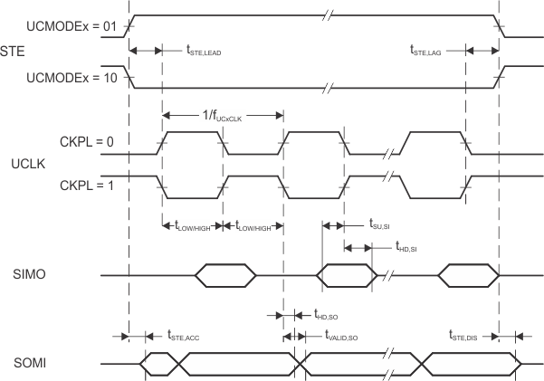
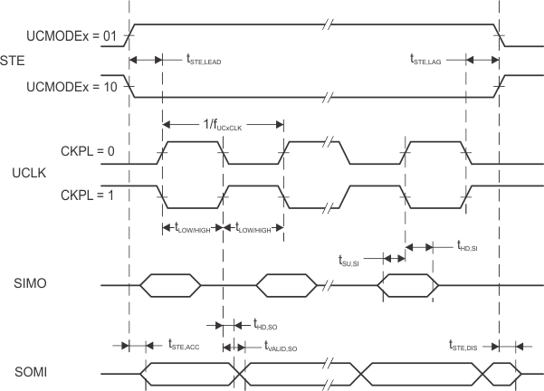
Table 5-18 eUSCI (SPI Slave Mode)
over recommended ranges of supply voltage and operating free-air temperature (unless otherwise noted)(1)| PARAMETER | TEST CONDITIONS | VCC | MIN | MAX | UNIT | |
|---|---|---|---|---|---|---|
| tSTE,LEAD | STE lead time, STE active to clock | 2 V | 55 | ns | ||
| 3 V | 45 | |||||
| tSTE,LAG | STE lag time, Last clock to STE inactive | 2 V | 20 | ns | ||
| 3 V | 20 | |||||
| tSTE,ACC | STE access time, STE active to SOMI data out | 2 V | 65 | ns | ||
| 3 V | 40 | |||||
| tSTE,DIS | STE disable time, STE inactive to SOMI high impedance | 2 V | 40 | ns | ||
| 3 V | 35 | |||||
| tSU,SI | SIMO input data setup time | 2 V | 8 | ns | ||
| 3 V | 6 | |||||
| tHD,SI | SIMO input data hold time | 2 V | 12 | ns | ||
| 3 V | 12 | |||||
| tVALID,SO | SOMI output data valid time(2) | UCLK edge to SOMI valid,
CL = 20 pF |
2 V | 68 | ns | |
| 3 V | 42 | |||||
| tHD,SO | SOMI output data hold time (3) | CL = 20 pF | 2 V | 5 | ns | |
| 3 V | 5 | |||||
(1) fUCxCLK = 1/2tLO/HI with tLO/HI ≥ max(tVALID,MO(Master) + tSU,SI(eUSCI), tSU,MI(Master) + tVALID,SO(eUSCI))
For the master parameters tSU,MI(Master) and tVALID,MO(Master), see the SPI parameters of the attached master.
For the master parameters tSU,MI(Master) and tVALID,MO(Master), see the SPI parameters of the attached master.
(2) Specifies the time to drive the next valid data to the SOMI output after the output changing UCLK clock edge. See the timing diagrams in Figure 5-15 and Figure 5-16.
(3) Specifies how long data on the SOMI output is valid after the output changing UCLK clock edge. See the timing diagrams in Figure 5-15 and Figure 5-16.
 Figure 5-15 SPI Slave Mode, CKPH = 0
  Figure 5-16 SPI Slave Mode, CKPH = 1
 Table 5-19 lists the characteristics of the eUSCI in I2C mode.