SLAS942E November 2015 – December 2019 MSP430FR2532 , MSP430FR2533 , MSP430FR2632 , MSP430FR2633
PRODUCTION DATA.
- 1Device Overview
- 2Revision History
- 3Device Comparison
- 4Terminal Configuration and Functions
-
5Specifications
- 5.1 Absolute Maximum Ratings
- 5.2 ESD Ratings
- 5.3 Recommended Operating Conditions
- 5.4 Active Mode Supply Current Into VCC Excluding External Current
- 5.5 Active Mode Supply Current Per MHz
- 5.6 Low-Power Mode LPM0 Supply Currents Into VCC Excluding External Current
- 5.7 Low-Power Mode (LPM3 and LPM4) Supply Currents (Into VCC) Excluding External Current
- 5.8 Low-Power Mode LPMx.5 Supply Currents (Into VCC) Excluding External Current
- 5.9 Typical Characteristics - Low-Power Mode Supply Currents
- Table 5-1 Typical Characteristics – Current Consumption Per Module
- 5.10 Thermal Resistance Characteristics
- 5.11 Timing and Switching Characteristics
-
6Detailed Description
- 6.1 Overview
- 6.2 CPU
- 6.3 Operating Modes
- 6.4 Interrupt Vector Addresses
- 6.5 Bootloader (BSL)
- 6.6 JTAG Standard Interface
- 6.7 Spy-Bi-Wire Interface (SBW)
- 6.8 FRAM
- 6.9 Memory Protection
- 6.10
Peripherals
- 6.10.1 Power-Management Module (PMM)
- 6.10.2 Clock System (CS) and Clock Distribution
- 6.10.3 General-Purpose Input/Output Port (I/O)
- 6.10.4 Watchdog Timer (WDT)
- 6.10.5 System (SYS) Module
- 6.10.6 Cyclic Redundancy Check (CRC)
- 6.10.7 Enhanced Universal Serial Communication Interface (eUSCI_A0, eUSCI_B0)
- 6.10.8 Timers (Timer0_A3, Timer1_A3, Timer2_A2 and Timer3_A2)
- 6.10.9 Hardware Multiplier (MPY)
- 6.10.10 Backup Memory (BAKMEM)
- 6.10.11 Real-Time Clock (RTC)
- 6.10.12 10-Bit Analog-to-Digital Converter (ADC)
- 6.10.13 CapTIvate Technology
- 6.10.14 Embedded Emulation Module (EEM)
- 6.11 Input/Output Diagrams
- 6.12 Device Descriptors
- 6.13 Memory
- 6.14 Identification
- 7Applications, Implementation, and Layout
- 8Device and Documentation Support
- 9Mechanical, Packaging, and Orderable Information
Package Options
Mechanical Data (Package|Pins)
Thermal pad, mechanical data (Package|Pins)
- RGE|24
Orderable Information
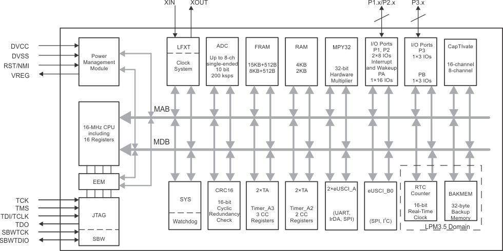
1.4 Functional Block Diagram
Figure 1-1 shows the functional block diagram.
 Figure 1-1 Functional Block Diagram
 - The MCU has one main power pair of DVCC and DVSS that supplies digital and analog modules. Recommended bypass and decoupling capacitors are 4.7 µF to 10 µF and 0.1 µF, respectively, with ±5% accuracy.
- VREG is the decoupling capacitor of the CapTIvate regulator. The recommended value for the required decoupling capacitor is 1 µF, with a maximum ESR of ≤200 mΩ.
- P1 and P2 feature the pin interrupt function and can wake the MCU from all LPMs, including LPM3.5 and LPM4.
- Each Timer_A3 has three capture/compare registers. Only CCR1 and CCR2 are externally connected. CCR0 registers can be used only for internal period timing and interrupt generation.
- Each Timer_A2 has two capture/compare registers. Both registers can be used only for internal period timing and interrupt generation.
- In LPM3 mode, the CapTIvate module can be functional while the rest of the peripherals are off.