SLAS942E November 2015 – December 2019 MSP430FR2532 , MSP430FR2533 , MSP430FR2632 , MSP430FR2633
PRODUCTION DATA.
- 1Device Overview
- 2Revision History
- 3Device Comparison
- 4Terminal Configuration and Functions
-
5Specifications
- 5.1 Absolute Maximum Ratings
- 5.2 ESD Ratings
- 5.3 Recommended Operating Conditions
- 5.4 Active Mode Supply Current Into VCC Excluding External Current
- 5.5 Active Mode Supply Current Per MHz
- 5.6 Low-Power Mode LPM0 Supply Currents Into VCC Excluding External Current
- 5.7 Low-Power Mode (LPM3 and LPM4) Supply Currents (Into VCC) Excluding External Current
- 5.8 Low-Power Mode LPMx.5 Supply Currents (Into VCC) Excluding External Current
- 5.9 Typical Characteristics - Low-Power Mode Supply Currents
- Table 5-1 Typical Characteristics – Current Consumption Per Module
- 5.10 Thermal Resistance Characteristics
- 5.11 Timing and Switching Characteristics
-
6Detailed Description
- 6.1 Overview
- 6.2 CPU
- 6.3 Operating Modes
- 6.4 Interrupt Vector Addresses
- 6.5 Bootloader (BSL)
- 6.6 JTAG Standard Interface
- 6.7 Spy-Bi-Wire Interface (SBW)
- 6.8 FRAM
- 6.9 Memory Protection
- 6.10
Peripherals
- 6.10.1 Power-Management Module (PMM)
- 6.10.2 Clock System (CS) and Clock Distribution
- 6.10.3 General-Purpose Input/Output Port (I/O)
- 6.10.4 Watchdog Timer (WDT)
- 6.10.5 System (SYS) Module
- 6.10.6 Cyclic Redundancy Check (CRC)
- 6.10.7 Enhanced Universal Serial Communication Interface (eUSCI_A0, eUSCI_B0)
- 6.10.8 Timers (Timer0_A3, Timer1_A3, Timer2_A2 and Timer3_A2)
- 6.10.9 Hardware Multiplier (MPY)
- 6.10.10 Backup Memory (BAKMEM)
- 6.10.11 Real-Time Clock (RTC)
- 6.10.12 10-Bit Analog-to-Digital Converter (ADC)
- 6.10.13 CapTIvate Technology
- 6.10.14 Embedded Emulation Module (EEM)
- 6.11 Input/Output Diagrams
- 6.12 Device Descriptors
- 6.13 Memory
- 6.14 Identification
- 7Applications, Implementation, and Layout
- 8Device and Documentation Support
- 9Mechanical, Packaging, and Orderable Information
Package Options
Mechanical Data (Package|Pins)
Thermal pad, mechanical data (Package|Pins)
- RHB|32
Orderable Information
6.11.4 Port P3 (P3.0 to P3.2) Input/Output With Schmitt Trigger
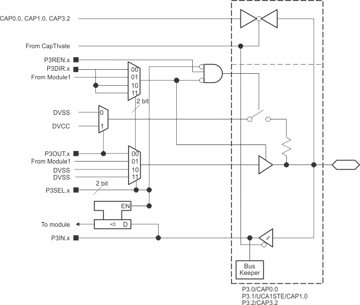
Figure 6-4 shows the port diagram. Table 6-20 summarizes the selection of pin function.
 Figure 6-4 Port P3 (P3.0 to P3.2) Input/Output With Schmitt Trigger
 NOTE
CapTIvate shared with I/Os configuration
The CapTIvate function and GPIOs are powered by different power supplies (1.5 V and 3.3 V, respectively).
To prevent pad damage when changing the function, TI recommends checking the external application circuit of each pad before enabling the alternate function.
Table 6-20 Port P3 (P3.0 to P3.2) Pin Functions
| PIN NAME (P3.x) | x | FUNCTION | CONTROL BITS AND SIGNALS(2) | ||
|---|---|---|---|---|---|
| P3DIR.x | P3SEL.x | ANALOG FUNCTION | |||
| P3.0/CAP0.0 | 0 | P3.0 (I/O) | I: 0; O: 1 | 00 | 0 |
| CAP0.0 | X | X | 1 | ||
| P3.1/UCA1STE/ CAP1.0 | 1 | P3.1 (I/O) | I: 0; O: 1 | 00 | 0 |
| UCA1STE | X | 01 | 0 | ||
| CAP1.0 | X | X | 1 | ||
| P3.2/CAP3.2 | 2 | P3.2 (I/O) | I: 0; O: 1 | 00 | 0 |
| CAP3.2 | X | X | 1 | ||