SLAS887C September 2014 – March 2021
PRODUCTION DATA
- 1 Features
- 2 Applications
- 3 Description
- 4 Functional Block Diagram
- 5 Revision History
- 6 Device Comparison
- 7 Terminal Configuration and Functions
-
8 Specifications
- 8.1 Absolute Maximum Ratings
- 8.2 ESD Ratings
- 8.3 Recommended Operating Conditions
- 8.4 Active Mode Supply Current (Into VCC) Excluding External Current
- 8.5 Low-Power Mode Supply Currents (Into VCC) Excluding External Current
- 8.6 Thermal Resistance Characteristics
- 8.7
Timing and Switching Characteristics
- 8.7.1 Reset Timing
- 8.7.2 Clock Specifications
- 8.7.3 Wake-up Characteristics
- 8.7.4 I/O Ports
- 8.7.5 Power Management Module
- 8.7.6 Reference Module
- 8.7.7
SD24
- 8.7.7.1 SD24 Power Supply and Recommended Operating Conditions
- 8.7.7.2 SD24 Internal Voltage Reference
- 8.7.7.3 SD24 External Voltage Reference
- 8.7.7.4 SD24 Input Range
- 8.7.7.5 SD24 Performance, Internal Reference (SD24REFS = 1, SD24OSRx = 256)
- 8.7.7.6 SD24 Performance, External Reference (SD24REFS = 0, SD24OSRx = 256)
- 8.7.7.7 Typical Characteristics
- 8.7.8 eUSCI
- 8.7.9 Timer_A
- 8.7.10 Flash
- 8.7.11 Emulation and Debug
- 9 Detailed Description
- 10Applications, Implementation, and Layout
- 11Device and Documentation Support
- 12Mechanical, Packaging, and Orderable Information
Package Options
Mechanical Data (Package|Pins)
Thermal pad, mechanical data (Package|Pins)
- RHB|32
Orderable Information
8.7.8.4 eUSCI (SPI Master Mode) Timing
over recommended ranges of supply voltage and operating free-air temperature (unless otherwise noted)(1)
| PARAMETER | TEST CONDITIONS | VCC | MIN | MAX | UNIT | |
|---|---|---|---|---|---|---|
| tSTE,LEAD | STE lead time, STE active to clock | UCSTEM = 1, UCMODEx = 01 or 10 | 2.2 V, 3 V | 150 | ns | |
| tSTE,LAG | STE lag time, Last clock to STE inactive | UCSTEM = 1, UCMODEx = 01 or 10 | 2.2 V, 3 V | 200 | ns | |
| tSTE,ACC | STE access time, STE active to SIMO data out | UCSTEM = 0, UCMODEx = 01 or 10 | 2.2 V | 40 | ns | |
| 3 V | 30 | |||||
| tSTE,DIS | STE disable time, STE inactive to SIMO high impedance | UCSTEM = 0, UCMODEx = 01 or 10 | 2.2 V | 40 | ns | |
| 3 V | 30 | |||||
| tSU,MI | SOMI input data setup time | 2.2 V | 50 | ns | ||
| 3 V | 30 | |||||
| tHD,MI | SOMI input data hold time | 2.2 V, 3 V | 0 | ns | ||
| tVALID,MO | SIMO output data valid time(2) | UCLK edge to SIMO valid, CL = 20 pF | 2.2 V | 7 | ns | |
| 3 V | 5 | |||||
| tHD,MO | SIMO output data hold time(3) | CL = 20 pF | 2.2 V, 3 V | 0 | ns | |
(1) fUCxCLK = 1/2tLO/HI with tLO/HI = max(tVALID,MO(eUSCI) + tSU,SI(Slave), tSU,MI(eUSCI) + tVALID,SO(Slave))
For the slave parameters tSU,SI(Slave) and tVALID,SO(Slave), refer to the SPI parameters of the attached slave.
For the slave parameters tSU,SI(Slave) and tVALID,SO(Slave), refer to the SPI parameters of the attached slave.
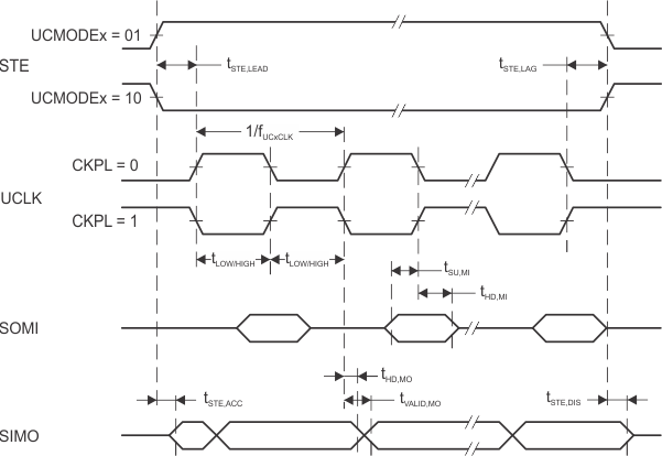
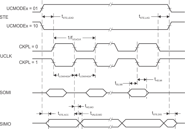
(2) Specifies the time to drive the next valid data to the SIMO output after the output changing UCLK clock edge. Refer to the timing diagrams in Figure 8-10 and Figure 8-11.
(3) Specifies how long data on the SIMO output is valid after the output changing UCLK clock edge. Negative values indicate that the data on the SIMO output can become invalid before the output changing clock edge observed on UCLK. Refer to the timing diagrams in Figure 8-10 and Figure 8-11.
 Figure 8-10 SPI Master Mode, CKPH = 0
 Figure 8-11 SPI Master Mode, CKPH = 1