SLAS887C September   2014  – March 2021

PRODUCTION DATA  

  1. Features
  2. Applications
  3. Description
  4. Functional Block Diagram
  5. Revision History
  6. Device Comparison
    1. 6.1 Related Products
  7. Terminal Configuration and Functions
    1. 7.1 Pin Diagrams
    2. 7.2 Signal Descriptions
    3. 7.3 Pin Multiplexing
    4. 7.4 Connection of Unused Pins
  8. Specifications
    1. 8.1 Absolute Maximum Ratings
    2. 8.2 ESD Ratings
    3. 8.3 Recommended Operating Conditions
    4. 8.4 Active Mode Supply Current (Into VCC) Excluding External Current
    5. 8.5 Low-Power Mode Supply Currents (Into VCC) Excluding External Current
    6. 8.6 Thermal Resistance Characteristics
    7. 8.7 Timing and Switching Characteristics
      1. 8.7.1  Reset Timing
        1. 8.7.1.1 Reset Timing
      2. 8.7.2  Clock Specifications
        1. 8.7.2.1 DCO in External Resistor Mode
        2. 8.7.2.2 DCO in Internal Resistor Mode
        3. 8.7.2.3 DCO Overall Tolerance Table
        4. 8.7.2.4 DCO in Bypass Mode Recommended Operating Conditions
      3. 8.7.3  Wake-up Characteristics
        1. 8.7.3.1 Wake-up Times From Low Power Modes
      4. 8.7.4  I/O Ports
        1. 8.7.4.1 Schmitt-Trigger Inputs – General-Purpose I/O
        2. 8.7.4.2 Inputs – Ports P1 and P2
        3. 8.7.4.3 Leakage Current – General-Purpose I/O
        4. 8.7.4.4 Outputs – General-Purpose I/O
        5. 8.7.4.5 Output Frequency – General-Purpose I/O
        6. 8.7.4.6 Typical Characteristics – Outputs
      5. 8.7.5  Power Management Module
        1. 8.7.5.1 PMM, High-Side Brownout Reset (BORH)
        2. 8.7.5.2 PMM, Low-Side SVS (SVSL)
        3. 8.7.5.3 PMM, Core Voltage
        4. 8.7.5.4 PMM, Voltage Monitor (VMON)
      6. 8.7.6  Reference Module
        1. 8.7.6.1 Voltage Reference (REF)
        2. 8.7.6.2 Temperature Sensor
      7. 8.7.7  SD24
        1. 8.7.7.1 SD24 Power Supply and Recommended Operating Conditions
        2. 8.7.7.2 SD24 Internal Voltage Reference
        3. 8.7.7.3 SD24 External Voltage Reference
        4. 8.7.7.4 SD24 Input Range
        5. 8.7.7.5 SD24 Performance, Internal Reference (SD24REFS = 1, SD24OSRx = 256)
        6. 8.7.7.6 SD24 Performance, External Reference (SD24REFS = 0, SD24OSRx = 256)
        7. 8.7.7.7 Typical Characteristics
      8. 8.7.8  eUSCI
        1. 8.7.8.1 eUSCI (UART Mode) Clock Frequency
        2. 8.7.8.2 eUSCI (UART Mode) Deglitch Characteristics
        3. 8.7.8.3 eUSCI (SPI Master Mode) Clock Frequency
        4. 8.7.8.4 eUSCI (SPI Master Mode) Timing
        5. 8.7.8.5 eUSCI (SPI Slave Mode) Timing
        6. 8.7.8.6 eUSCI (I2C Mode) Timing
      9. 8.7.9  Timer_A
        1. 8.7.9.1 Timer_A
      10. 8.7.10 Flash
        1. 8.7.10.1 Flash Memory
      11. 8.7.11 Emulation and Debug
        1. 8.7.11.1 JTAG and Spy-Bi-Wire Interface
  9. Detailed Description
    1. 9.1  Overview
    2. 9.2  Functional Block Diagrams
    3. 9.3  CPU
    4. 9.4  Instruction Set
    5. 9.5  Operating Modes
    6. 9.6  Interrupt Vector Addresses
    7. 9.7  Special Function Registers
    8. 9.8  Flash Memory
    9. 9.9  JTAG Operation
      1. 9.9.1 JTAG Standard Interface
      2. 9.9.2 Spy-Bi-Wire Interface
      3. 9.9.3 JTAG Disable Register
    10. 9.10 Peripherals
      1. 9.10.1 Clock System
      2. 9.10.2 Power-Management Module (PMM)
      3. 9.10.3 Digital I/O
      4. 9.10.4 Watchdog Timer (WDT)
      5. 9.10.5 Timer TA0
      6. 9.10.6 Timer TA1
      7. 9.10.7 Enhanced Universal Serial Communication Interface (eUSCI)
      8. 9.10.8 Hardware Multiplier
      9. 9.10.9 SD24
    11. 9.11 Input/Output Diagrams
      1. 9.11.1 Port P1, P1.0 to P1.3, Input/Output With Schmitt Trigger
      2. 9.11.2 Port P1, P1.4 to P1.7, Input/Output With Schmitt Trigger
      3. 9.11.3 Port P2, P2.0 to P2.2 and P2.4 to P2.7, Input/Output With Schmitt Trigger
      4. 9.11.4 Port P2, P2.3, Input/Output With Schmitt Trigger
    12. 9.12 Device Descriptor
    13. 9.13 Memory
      1. 9.13.1 Peripheral File Map
    14. 9.14 Identification
      1. 9.14.1 Device Identification
      2. 9.14.2 JTAG Identification
  10. 10Applications, Implementation, and Layout
  11. 11Device and Documentation Support
    1. 11.1 Getting Started and Next Steps
    2. 11.2 Device Nomenclature
    3. 11.3 Tools and Software
    4. 11.4 Documentation Support
    5. 11.5 Support Resources
    6. 11.6 Trademarks
    7. 11.7 Electrostatic Discharge Caution
    8. 11.8 Glossary
  12. 12Mechanical, Packaging, and Orderable Information

Package Options

Mechanical Data (Package|Pins)
Thermal pad, mechanical data (Package|Pins)
Orderable Information

Recommended Operating Conditions

MIN NOM MAX UNIT
VCC Supply voltage during program execution and flash programming or erase (VCC = VCC) 2.2 3.6 V
VSS Supply voltage (AVSS  = DVSS = VSS) 0 V
TA Operating free-air temperature T temperature range –40 105 °C
TJ Operating junction temperature T temperature range –40 105 °C
CVCORE Recommended capacitor at VCORE 470 nF
CVCC/
CVCORE
Capacitor ratio of VCC to VCORE 10
fSYSTEM Processor frequency (maximum MCLK frequency) (1) (2) 0 16.384 MHz
The MSP430i CPU is clocked directly with MCLK.
Modules may have a different maximum input clock specification. See the specification of the respective module in this data sheet.
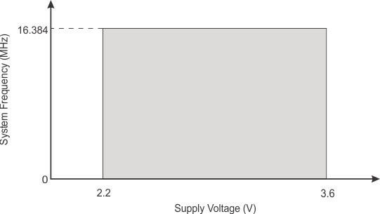
GUID-20210108-CA0I-RBSS-ZFLH-FLXPCNTVQDGB-low.gif Figure 8-1 Maximum System Frequency