SBAS758C January 2016 – September 2016 MUX508 , MUX509
PRODUCTION DATA.
- 1 Features
- 2 Applications
- 3 Description
- 4 Revision History
- 5 Device Comparison Table
- 6 Pin Configuration and Functions
- 7 Specifications
- 8 Parameter Measurement Information
- 9 Detailed Description
- 10Applications and Implementation
- 11Power-Supply Recommendations
- 12Layout
- 13Device and Documentation Support
- 14Mechanical, Packaging, and Orderable Information
Package Options
Mechanical Data (Package|Pins)
Thermal pad, mechanical data (Package|Pins)
Orderable Information
9 Detailed Description
9.1 Overview
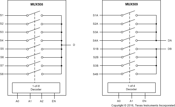
The MUX50x are a family of analog multiplexers. The Functional Block Diagram section provides a top-level block diagram of both the MUX508 and MUX509. The MUX508 is an eight-channel, single-ended, analog mux. The MUX509 is a four-channel, differential or dual 4:1, single-ended, analog mux. Each channel is turned on or turned off based on the state of the address lines and enable pin.
9.2 Functional Block Diagram
9.3 Feature Description
9.3.1 Ultralow Leakage Current
The MUX50x provide extremely low on- and off-leakage currents. The MUX50x are capable of switching signals from high source-impedance inputs into a high input-impedance op amp with minimal offset error because of these ultralow leakage currents. Figure 37 shows typical leakage currents of the MUX50x versus temperature.
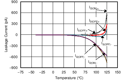 Figure 37. Leakage Current vs Temperature
9.3.2 Ultralow Charge Injection
The MUX50x have a simple transmission gate topology, as shown in Figure 38. Any mismatch in the stray capacitance associated with the NMOS and PMOS transistors creates an output level change whenever the switch is opened or closed.
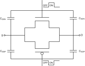 Figure 38. Transmission Gate Topology
The MUX50x have special charge-injection cancellation circuitry that reduces the source-to-drain charge injection to as low as 0.3 pC at VS = 0 V, and ±0.6 pC in the full signal range, as shown in Figure 39.
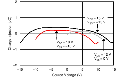 Figure 39. Source-to-Drain Charge Injection vs Source or Drain voltage
The drain-to-source charge injection becomes important when the device is used as a demultiplexer (demux), where D becomes the input and Sx becomes the output. Figure 40 shows the drain-to-source charge injection across the full signal range.
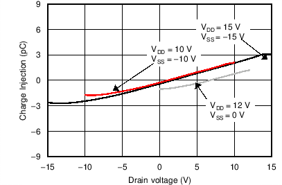 Figure 40. Drain-to-Source Charge Injection vs Source or Drain voltage
9.3.3 Bidirectional Operation
The MUX50x are operable as both a mux or demux. The source (Sx, SxA, SxB) and drain (D, DA, DB) pins of the MUX50x are used either as input or output. Each MUX50x channel has very similar characteristics in both directions.
9.3.4 Rail-to-Rail Operation
A valid analog signal for the MUX50x ranges from VSS to VDD. The input signal to the MUX50x can swing from VSS to VDD without any significant degradation in performance. The on-resistance of the MUX50x varies with input signal, as shown in Figure 41.
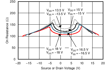 Figure 41. On-Resistance vs Source or Drain Voltage
9.4 Device Functional Modes
When the EN pin of the MUX50x is pulled high, one of the switches is closed based on the state of the address lines. When the EN pin is pulled low, all the switches are in an open state irrespective of the state of the address lines. The EN pin can be connected to VDD (as high as 36 V).