SBAS758C January   2016  – September 2016 MUX508 , MUX509

PRODUCTION DATA.  

  1. Features
  2. Applications
  3. Description
  4. Revision History
  5. Device Comparison Table
  6. Pin Configuration and Functions
  7. Specifications
    1. 7.1 Absolute Maximum Ratings
    2. 7.2 ESD Ratings
    3. 7.3 Recommended Operating Conditions
    4. 7.4 Thermal Information
    5. 7.5 Electrical Characteristics: Dual Supply
    6. 7.6 Electrical Characteristics: Single Supply
    7. 7.7 Typical Characteristics
  8. Parameter Measurement Information
    1. 8.1  Truth Tables
    2. 8.2  On-Resistance
    3. 8.3  Off-Leakage Current
    4. 8.4  On-Leakage Current
    5. 8.5  Transition Time
    6. 8.6  Break-Before-Make Delay
    7. 8.7  Turn-On and Turn-Off Time
    8. 8.8  Charge Injection
    9. 8.9  Off Isolation
    10. 8.10 Channel-to-Channel Crosstalk
    11. 8.11 Bandwidth
    12. 8.12 THD + Noise
  9. Detailed Description
    1. 9.1 Overview
    2. 9.2 Functional Block Diagram
    3. 9.3 Feature Description
      1. 9.3.1 Ultralow Leakage Current
      2. 9.3.2 Ultralow Charge Injection
      3. 9.3.3 Bidirectional Operation
      4. 9.3.4 Rail-to-Rail Operation
    4. 9.4 Device Functional Modes
  10. 10Applications and Implementation
    1. 10.1 Application Information
    2. 10.2 Typical Application
      1. 10.2.1 Design Requirements
      2. 10.2.2 Detailed Design Procedure
      3. 10.2.3 Application Curve
  11. 11Power-Supply Recommendations
  12. 12Layout
    1. 12.1 Layout Guidelines
    2. 12.2 Layout Example
  13. 13Device and Documentation Support
    1. 13.1 Documentation Support
      1. 13.1.1 Related Documentation
    2. 13.2 Related Links
    3. 13.3 Receiving Notification of Documentation Updates
    4. 13.4 Community Resources
    5. 13.5 Trademarks
    6. 13.6 Electrostatic Discharge Caution
    7. 13.7 Glossary
  14. 14Mechanical, Packaging, and Orderable Information

Package Options

Mechanical Data (Package|Pins)
Thermal pad, mechanical data (Package|Pins)
Orderable Information

11 Power-Supply Recommendations

The MUX50x operates across a wide supply range of ±5 V to ±18 V (10 V to 36 V in single-supply mode). The MUX508 and MUX509 operate equally well with either dual supplies (±5 V to ±18 V), or a single supply (10 V to 36 V). They also perform well with unsymmetric supplies such as VDD = 12 V and VSS = –5 V. For reliable operation, use a supply decoupling capacitor with a capacitance between 0.1 µF to 10 µF at both the VDD and VSS pins to ground.

The on-resistance of the MUX50x varies with supply voltage, as shown in Figure 44.
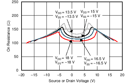
MUX508 MUX509 C001_SBOS705.png Figure 44. On-Resistance Variation With Supply and Input Voltage