SLLSEO4A June 2015 – July 2015 ONET1130EP
PRODUCTION DATA.
- 1 Features
- 2 Applications
- 3 Description
- 4 Revision History
- 5 Description (continued)
- 6 Pin Configuration and Function
- 7 Specifications
-
8 Detailed Description
- 8.1 Overview
- 8.2 Functional Block Diagram
- 8.3 Feature Description
- 8.4 Device Functional Modes
- 8.5 Programming
- 8.6
Register Mapping
- 8.6.1 R/W Control Registers
- 8.6.2
RX Registers
- 8.6.2.1 RX Register 4 (offset = 0000 0000) [reset = 0h]
- 8.6.2.2 RX Register 5 (offset = 0000 0000) [reset = 0h]
- 8.6.2.3 RX Register 6 (offset = 0000 0000) [reset = 0h]
- 8.6.2.4 RX Register 7 (offset = 0000 0000) [reset = 0h]
- 8.6.2.5 RX Register 8 (offset = 0000 0000) [reset = 0h]
- 8.6.2.6 RX Register 9 (offset = 0000 0000) [reset = 0h]
- 8.6.3
TX Registers
- 8.6.3.1 TX Register 10 (offset = 0000 0000) [reset = 0h]
- 8.6.3.2 TX Register 11 (offset = 0000 0000) [reset = 0h]
- 8.6.3.3 TX Register 12 (offset = 0000 0000) [reset = 0h]
- 8.6.3.4 TX Register 13 (offset = 0h) [reset = 0]
- 8.6.3.5 TX Register 14 (offset = 0000 0000) [reset = 0h]
- 8.6.3.6 TX Register 15 (offset = 0000 0000) [reset = 0h]
- 8.6.3.7 TX Register 16 (offset = 0000 0000) [reset = 0h]
- 8.6.3.8 TX Register 17 (offset = 0000 0000) [reset = 0h]
- 8.6.3.9 TX Register 18 (offset = 0000 0000) [reset = 0h]
- 8.6.4 Reserved Registers
- 8.6.5 Read Only Registers
- 8.6.6 Adjustment Registers
- 9 Application Information and Implementations
- 10Power Supply Recommendations
- 11Layout
- 12Device and Documentation Support
- 13Mechanical, Packaging, and Orderable Information
Package Options
Mechanical Data (Package|Pins)
- RSM|32
Thermal pad, mechanical data (Package|Pins)
- RSM|32
Orderable Information
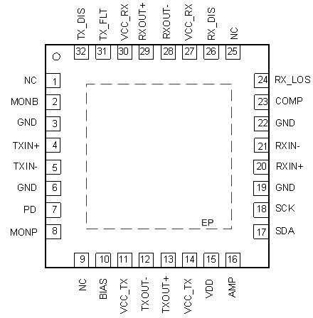
6 Pin Configuration and Function
RSM PACKAGE
32 PIN VQFN
(TOP VIEW)

Pin Functions
| NUMBER | NAME | Type | DESCRIPTION |
|---|---|---|---|
| AMP | 16 | Analog-in | Output amplitude control. Output amplitude can be adjusted by applying a voltage of 0 to 2 V to this pin. Leave open when not used. |
| BIAS | 10 | Analog | Sinks or sources the bias current for the laser in both APC and open loop modes. |
| COMP | 23 | Analog | Compensation pin used to control the bandwidth of the APC loop. Connect a 0.01-µF capacitor to ground. |
| GND | 3, 6, 19, 22 | Supply | Circuit ground. |
| MONB | 2 | Analog-out | Bias current monitor. |
| MONP | 8 | Analog-out | Photodiode current monitor. |
| NC | 1, 9, 25 | Do not connect. | |
| PD | 7 | Analog | Photodiode input. Pin can source or sink current dependent on register setting. |
| RX_DIS | 26 | Digital-in | Disables the receiver output buffer when set to a high level. Includes a 250-kΩ pull-up resistor to VCC. Ground the pin to enable the output. This is an ORed function with the RXOUT_DIS bit (bit 6 in register 4). This pin is 3.3-V tolerant. |
| RX_LOS | 24 | Digital-out | Receiver loss of signal. High level indicates that the receiver input signal amplitude is below the programmed threshold level. Open drain output. Requires an external 4.7-kΩ to 10-kΩ pull-up resistor to VCC for proper operation. This pin is 3.3-V tolerant. |
| RXIN+ | 20 | Analog-in | Non-inverted receiver data input. On-chip differentially 100 Ω terminated to RXIN–. Must be AC coupled. |
| RXIN- | 21 | Analog-in | Inverted receiver data input. On-chip differentially 100 Ω terminated to RXIN+. Must be AC coupled. |
| RXOUT– | 28 | CML-out | Inverted receiver data output. 45 Ω back-terminated to VCC. |
| RXOUT+ | 29 | CML-out | Non-inverted data output. 45 Ω back-terminated to VCC. |
| SDA | 17 | Digital-in/out | 2-wire interface serial data input. Requires an external 4.7-kΩ to10-kΩ pull-up resistor to VCC. This pin is 3.3-V tolerant. |
| SCK | 18 | Digital-in | 2-wire interface serial clock input. Requires an external 4.7-kΩ to10-kΩ pull-up resistor to VCC. This pin is 3.3-V tolerant. |
| TX_DIS | 32 | Digital-in | Disables both bias and modulation currents when set to high state. Includes a 250-kΩ pull-up resistor to VCC. Requires an external 4.7 kΩ to 10 kΩ pull-up resistor to VCC for proper operation Toggle to reset a fault condition. This is an ORed function with the TXBIASEN bit (bit 2 in register 1). This pin is 3.3-V tolerant. |
| TXIN+ | 4 | Analog-in | Non-inverted transmitter data input. On-chip differentially 100 Ω terminated to TXIN–. Must be AC coupled. |
| TXIN– | 5 | Analog-in | Inverted transmitter data input. On-chip differentially 100 Ω terminated to TXIN+. Must be AC coupled. |
| TX_FLT | 31 | Digital-out | Transmitter fault detection flag. High level indicates that a fault has occurred. Open drain output. Requires an external 4.7 kΩ to 10 kΩ pull-up resistor to VCC for proper operation. This pin is 3.3-V tolerant. |
| TXOUT– | 12 | CML-out | Inverted transmitter data output. Internally terminated in single-ended operation mode. |
| TXOUT+ | 13 | CML-out | Non-Inverted transmitter data output. |
| VCC_RX | 27, 30 | Supply | 2.5 V ± 5% supply for the receiver. |
| VCC_TX | 11, 14 | Supply | 2.5 V ± 5% supply for the transmitter. |
| VDD | 15 | Supply | 2.5 V ± 5% supply for the digital circuitry. |
| Exposed Pad | EP | Exposed die pad. Solder to the PCB. |