SBOS040B November   1994  – July 2024 OPA131 , OPA2131 , OPA4131

PRODUCTION DATA  

  1.   1
  2. 1Features
  3. 2Applications
  4. 3Description
  5. 4Pin Configuration and Functions
  6. 5Specifications
    1. 5.1 Absolute Maximum Ratings
    2. 5.2 Recommended Operating Conditions
    3. 5.3 Thermal Information - OPA131
    4. 5.4 Thermal Information - OPA2131
    5. 5.5 Thermal Information - OPA4131
    6. 5.6 Electrical Characteristics
    7. 5.7 Typical Characteristics
  7. 6Application and Implementation
    1. 6.1 Application Information
      1. 6.1.1 Offset Voltage Trim
    2. 6.2 Typical Application
      1. 6.2.1 Input Bias Current
  8. 7Device and Documentation Support
    1. 7.1 Receiving Notification of Documentation Updates
    2. 7.2 Support Resources
    3. 7.3 Trademarks
    4. 7.4 Electrostatic Discharge Caution
    5. 7.5 Glossary
  9. 8Revision History
  10. 9Mechanical, Packaging, and Orderable Information

Package Options

Refer to the PDF data sheet for device specific package drawings

Mechanical Data (Package|Pins)
  • D|8
Thermal pad, mechanical data (Package|Pins)
Orderable Information

Typical Characteristics

at TA = 25°C, VS = ±15V, RL = 10kΩ connected to midsupply, and VCM = VOUT = midsupply (unless otherwise noted)
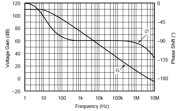
OPA131 OPA2131 OPA4131 Open-Loop Gain and Phase vs Frequency
 
Figure 5-1 Open-Loop Gain and Phase vs Frequency
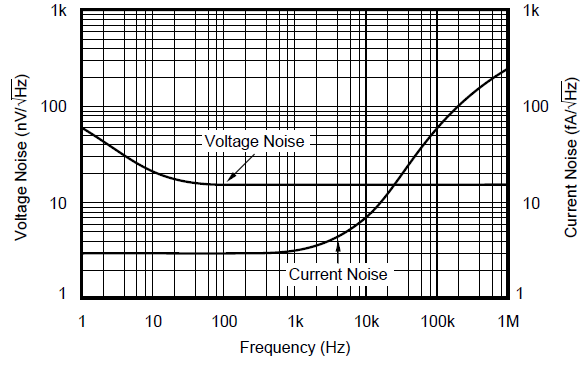
OPA131 OPA2131 OPA4131 Input
                        Voltage and Current Noise Spectral Density vs Frequency
 
Figure 5-3 Input Voltage and Current Noise Spectral Density vs Frequency
OPA131 OPA2131 OPA4131 Input
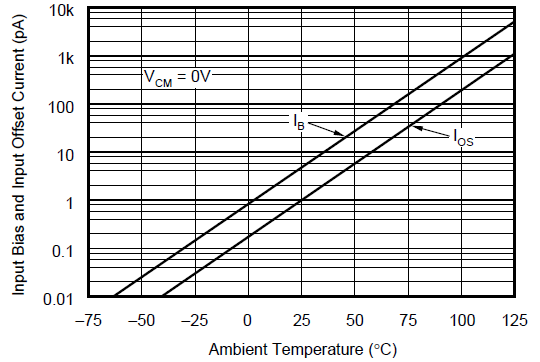
                        Bias and Input Offset Current vs Temperature
 
Figure 5-5 Input Bias and Input Offset Current vs Temperature
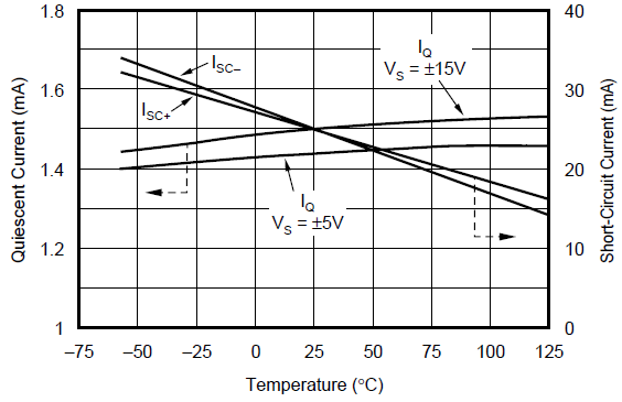
OPA131 OPA2131 OPA4131 Quiescent Current and
                        Short-Circuit Current vs Temperature
 
Figure 5-7 Quiescent Current and Short-Circuit Current vs Temperature
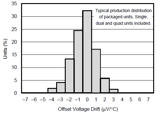
OPA131 OPA2131 OPA4131 Offset Voltage Drift
                        Production Distribution
 
Figure 5-9 Offset Voltage Drift Production Distribution
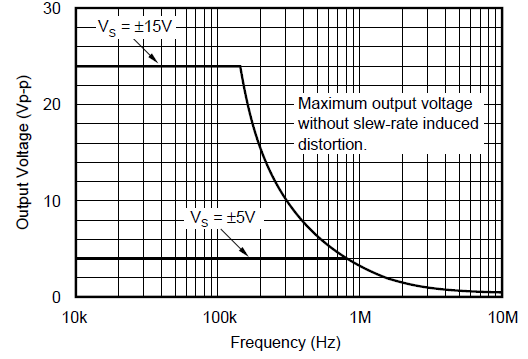
OPA131 OPA2131 OPA4131 Maximum Output Voltage vs
                        Frequency
 
Figure 5-11 Maximum Output Voltage vs Frequency
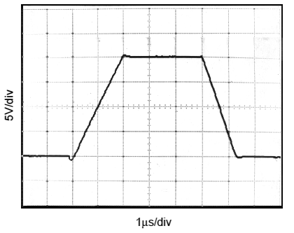
OPA131 OPA2131 OPA4131 Large-Signal Step Response
                        G = 1, CL = 300pF
 
Figure 5-13 Large-Signal Step Response G = 1, CL = 300pF
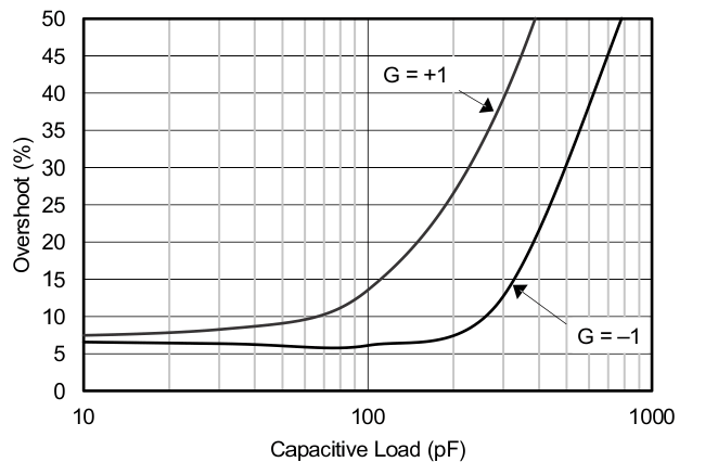
OPA131 OPA2131 OPA4131 Small-Signal Overshoot vs
                        Load Capacitance
 
Figure 5-15 Small-Signal Overshoot vs Load Capacitance
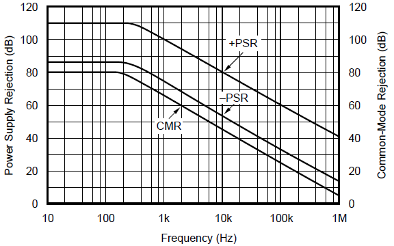
OPA131 OPA2131 OPA4131 Power
                        Supply and Common-Mode Rejection vs Frequency
 
Figure 5-2 Power Supply and Common-Mode Rejection vs Frequency
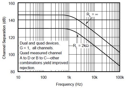
OPA131 OPA2131 OPA4131 Channel Separation vs Frequency
 
Figure 5-4 Channel Separation vs Frequency
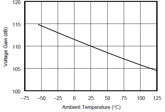
OPA131 OPA2131 OPA4131 Open-Loop Gain vs
                        Temperature
 
Figure 5-6 Open-Loop Gain vs Temperature
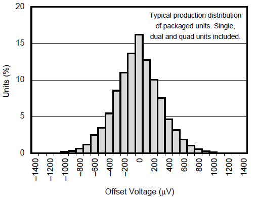
OPA131 OPA2131 OPA4131 Offset Voltage Production
                        Distribution
 
Figure 5-8 Offset Voltage Production Distribution
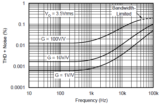
OPA131 OPA2131 OPA4131 Total Harmonic Distortion
                        + Noise vs Frequency
 
Figure 5-10 Total Harmonic Distortion + Noise vs Frequency
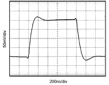
OPA131 OPA2131 OPA4131 Small-Signal Step Response
                        G = 1, CL = 300pF
 
Figure 5-12 Small-Signal Step Response G = 1, CL = 300pF
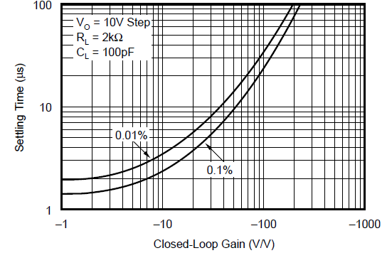
OPA131 OPA2131 OPA4131 Settling Time vs
                        Closed-Loop Gain
 
Figure 5-14 Settling Time vs Closed-Loop Gain
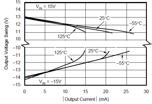
OPA131 OPA2131 OPA4131 Output Voltage Swing vs
                        Output Current
 
Figure 5-16 Output Voltage Swing vs Output Current