SBOSA00B December   2019  – August 2020 OPA1637

PRODUCTION DATA  

  1. Features
  2. Applications
  3. Description
  4. Revision History
  5. Pin Configuration and Functions
  6. Specifications
    1. 6.1 Absolute Maximum Ratings
    2. 6.2 ESD Ratings
    3. 6.3 Recommended Operating Conditions
    4. 6.4 Thermal Information
    5. 6.5 Electrical Characteristics
    6. 6.6 Typical Characteristics
  7. Parameter Measurement Information
    1. 7.1 Characterization Configuration
  8. Detailed Description
    1. 8.1 Overview
    2. 8.2 Functional Block Diagram
    3. 8.3 Feature Description
      1. 8.3.1 Super-Beta Input Bipolar Transistors
      2. 8.3.2 Power Down
      3. 8.3.3 Flexible Gain Setting
      4. 8.3.4 Amplifier Overload Power Limit
    4. 8.4 Device Functional Modes
  9. Application and Implementation
    1. 9.1 Application Information
      1. 9.1.1 Driving Capacitive Loads
      2. 9.1.2 Operating the Power-Down Feature
      3. 9.1.3 I/O Headroom Considerations
      4. 9.1.4 Noise Performance
    2. 9.2 Typical Applications
      1. 9.2.1 Current-Output Audio DAC Buffer to Class-D Amplifier
        1. 9.2.1.1 Design Requirements
        2. 9.2.1.2 Detailed Design Procedure
        3. 9.2.1.3 Application Curves
      2. 9.2.2 An MFB Filter Driving an ADC Application
        1. 9.2.2.1 Design Requirements
        2. 9.2.2.2 Detailed Design Procedure
        3. 9.2.2.3 Application Curves
      3. 9.2.3 Differential Microphone Input to Line Level
        1. 9.2.3.1 Application Curves
  10. 10Power Supply Recommendations
  11. 11Layout
    1. 11.1 Layout Guidelines
      1. 11.1.1 Board Layout Recommendations
    2. 11.2 Layout Example
  12. 12Device and Documentation Support
    1. 12.1 Device Support
      1. 12.1.1 Development Support
    2. 12.2 Documentation Support
      1. 12.2.1 Related Documentation
    3. 12.3 Receiving Notification of Documentation Updates
    4. 12.4 Support Resources
    5. 12.5 Trademarks
    6. 12.6 Electrostatic Discharge Caution
    7. 12.7 Glossary
  13. 13Mechanical, Packaging, and Orderable Information

Package Options

Mechanical Data (Package|Pins)
Thermal pad, mechanical data (Package|Pins)
Orderable Information

Pin Configuration and Functions

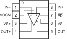
GUID-967CA48C-1001-4466-A393-EDB4FF3289E8-low.gifFigure 5-1 DGK Package, 8-Pin VSSOP, Top View
Pin Functions
PIN I/O DESCRIPTION
NAME NO.
IN– 1 I Inverting (negative) amplifier input
IN+ 8 I Noninverting (positive) amplifier input
OUT– 5 O Inverting (negative) amplifier output
OUT+ 4 O Noninverting (positive) amplifier output
PD 7 I Power down.
PD = logic low = power off mode.
PD = logic high = normal operation.
The logic threshold is referenced to VS+.
If power down is not needed, leave PD floating.
VOCM 2 I Ouput common-mode voltage control input
VS– 6 I Negative power-supply input
VS+ 3 I Positive power-supply input