SBOS489A December 2011 – December 2024 OPA1662 , OPA1664
PRODUCTION DATA
- 1
- 1Features
- 2Applications
- 3Description
- 4Pin Configurations
- 5Specifications
- 6Application and Implementation
- 7Device and Documentation Support
- 8Revision History
- 9Mechanical, Packaging, and Orderable Information
Package Options
Refer to the PDF data sheet for device specific package drawings
Mechanical Data (Package|Pins)
- D|8
- DGK|8
Thermal pad, mechanical data (Package|Pins)
Orderable Information
6.1.3 Noise Performance
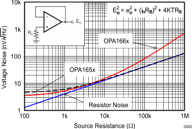
Figure 6-3 shows the total circuit noise for varying source impedance values with the op amp in a unity-gain configuration (no feedback resistor network, and therefore no additional noise contributions).
The OPA166x (GBW = 22MHz, G = +1) is shown with total circuit noise calculated. The op amp contributes both a voltage noise component and a current noise component. The voltage noise is commonly modeled as a time-varying component of the offset voltage. The current noise is modeled as the time-varying component of the input bias current and reacts with the source resistance to create a voltage component of noise. Therefore, the lowest noise op amp for a given application depends on the source impedance. For low source impedance, current noise is negligible, and voltage noise generally dominates. The low voltage noise of the OPA166x series op amps makes them a better choice for low source impedances of less than 1kΩ.
The equation in Figure 6-3 shows the calculation of the total circuit noise, with these parameters:
- en = Voltage noise
- in = Current noise
- RS = Source impedance
- k = Boltzmann’s constant = 1.38 × 10⁻²³ J/K
- T = Temperature in kelvins (K)
 Figure 6-3 Noise Performance of the OPA166x in Unity-Gain
Buffer Configuration