SBOS516H September 2010 – June 2024 OPA171 , OPA2171 , OPA4171
PRODUCTION DATA
- 1
- 1 Features
- 2 Applications
- 3 Description
- 4 Pin Configuration and Functions
- 5 Specifications
- 6 Detailed Description
- 7 Application and Implementation
- 8 Device and Documentation Support
- 9 Revision History
- 10Mechanical, Packaging, and Orderable Information
Package Options
Mechanical Data (Package|Pins)
Thermal pad, mechanical data (Package|Pins)
Orderable Information
6.3.4 Capacitive Load and Stability
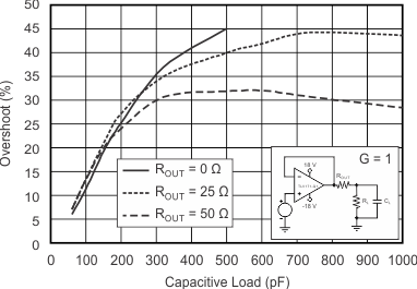
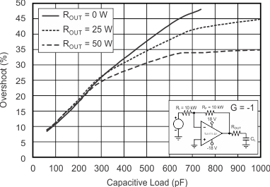
The dynamic characteristics of the OPAx171-Q1 family of devices have been optimized for commonly encountered operating conditions. The combination of low closed-loop gain and high capacitive loads decreases the phase margin of the amplifier and can lead to gain peaking or oscillations. As a result, heavier capacitive loads must be isolated from the output. The simplest way to achieve this isolation is to add a small resistor (for example, ROUT equal to 50 Ω) in series with the output. Figure 6-2 and Figure 6-3 show small-signal overshoot versus capacitive load for several values of ROUT. For details of analysis techniques and application circuits, see Applications Bulletin AB-028, available for download from TI.com.
 Figure 6-2 Small-Signal Overshoot vs Capacitive Load (100-mV Output Step)
 Figure 6-3 Small-Signal Overshoot vs Capacitive Load (100-mV Output Step)