SBOS584E November 2011 – June 2018 OPA180 , OPA2180 , OPA4180
PRODUCTION DATA.
- 1 Features
- 2 Applications
- 3 Description
- 4 Revision History
- 5 Device Comparison Table
- 6 Pin Configuration and Functions
-
7 Specifications
- 7.1 Absolute Maximum Ratings
- 7.2 ESD Ratings
- 7.3 Recommended Operating Conditions
- 7.4 Thermal Information: OPA180
- 7.5 Thermal Information: OPA2180
- 7.6 Thermal Information: OPA4180
- 7.7 Electrical Characteristics: VS = ±2 V to ±18 V (VS = 4 V to 36 V)
- 7.8 Typical Characteristics: Table of Graphs
- 7.9 Typical Characteristics
- 8 Detailed Description
- 9 Application and Implementation
- 10Power Supply Recommendations
- 11Layout
- 12Device and Documentation Support
- 13Mechanical, Packaging, and Orderable Information
Package Options
Mechanical Data (Package|Pins)
Thermal pad, mechanical data (Package|Pins)
Orderable Information
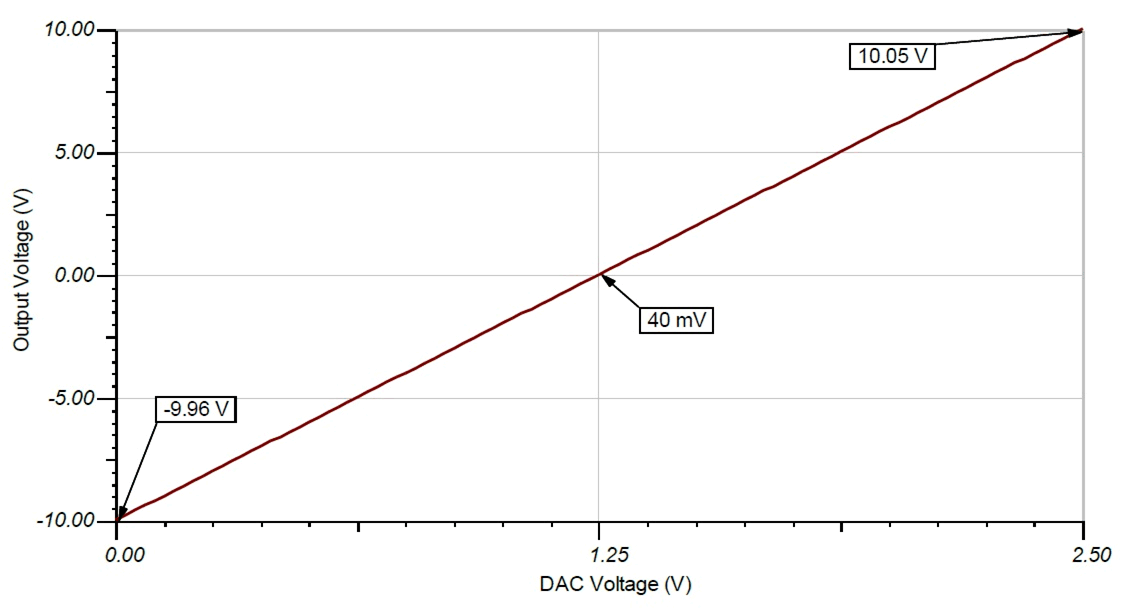
9.2.1.3 Application Curves
 Figure 31. Full-Scale Output Waveform
  Figure 32. DC Transfer Characteristic
 |
For step-by-step design procedure, circuit schematics, bill of materials, PCB files, simulation results, and test results, refer to TI Precision Design TIPD125, Bipolar ±10V Analog Output from a Unipolar Voltage Output DAC |