SBOS869 July 2017 OPA196 , OPA2196 , OPA4196
PRODUCTION DATA.
- 1 Features
- 2 Applications
- 3 Description
- 4 Revision History
- 5 Pin Configuration and Functions
-
6 Specifications
- 6.1 Absolute Maximum Ratings
- 6.2 ESD Ratings
- 6.3 Recommended Operating Conditions
- 6.4 Thermal Information: OPA196
- 6.5 Thermal Information: OPA2196
- 6.6 Thermal Information: OPA4196
- 6.7 Electrical Characteristics: VS = ±4 V to ±18 V (VS = 8 V to 36 V)
- 6.8 Electrical Characteristics: VS = ±2.25 V to ±4 V (VS = 4.5 V to 8 V)
- 6.9 Typical Characteristics
- 7 Detailed Description
- 8 Application and Implementation
- 9 Power-Supply Recommendations
- 10Layout
- 11Device and Documentation Support
- 12Mechanical, Packaging, and Orderable Information
Package Options
Mechanical Data (Package|Pins)
Thermal pad, mechanical data (Package|Pins)
Orderable Information
8 Application and Implementation
NOTE
Information in the following applications sections is not part of the TI component specification, and TI does not warrant its accuracy or completeness. TI’s customers are responsible for determining suitability of components for their purposes. Customers should validate and test their design implementation to confirm system functionality.
8.1 Application Information
The OPAx196 family offers outstanding dc precision and ac performance. These devices operate up to 36-V supply rails and offer true rail-to-rail input/output, ultralow offset voltage and offset voltage drift, as well as
2-MHz bandwidth and high capacitive load drive. These features make the OPAx196 a robust, high-performance operational amplifier for high-voltage industrial applications.
8.2 Typical Applications
8.2.1 Low-side Current Measurement
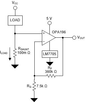
Figure 46 shows the OPA196 configured in a low-side current sensing application. For a full analysis of the circuit shown in Figure 46 including theory, calculations, simulations, and measured data see the 0-1A, single-supply, low-side, current sensing solution, see TIPD129.
 Figure 46. OPA196 in a Low-Side, Current-Sensing Application
 8.2.1.1 Design Requirements
The design requirements for this design are:
- Load current: 0 A to 1 A
- Output voltage: 4.9 V
- Maximum shunt voltage: 100 mV
8.2.1.2 Detailed Design Procedure
The transfer function of the circuit in Figure 46 is given in Equation 1:

The load current (ILOAD) produces a voltage drop across the shunt resistor (RSHUNT). The load current is set from 0 A to 1 A. To keep the shunt voltage below 100 mV at maximum load current, the largest shunt resistor is defined using Equation 2.

Using Equation 2, RSHUNT is calculated to be 100 mΩ. The voltage drop produced by ILOAD and RSHUNT is amplified by the OPA196 to produce an output voltage of 0 V to 4.9 V. The gain needed by the OPA196 to produce the necessary output voltage is calculated using Equation 3:

Using Equation 3, the required gain is calculated to be 49 V/V, which is set with resistors RF and RG. Equation 4 is used to size the resistors, RF and RG, to set the gain of the OPA196 to 49 V/V.

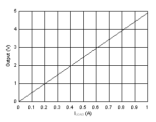
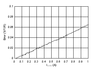
Choosing RF as 360 kΩ, RG is calculated to be 7.5 kΩ. RF and RG were chosen as 360 kΩ and 7.5 kΩ because they are standard value resistors that create a 49:1 ratio. Other resistors that create a 49:1 ratio can also be used. Figure 2 shows the measured transfer function of the circuit shown in Figure 46.
8.2.1.3 Application Curves


8.2.2 16-Bit Precision Multiplexed Data-Acquisition System
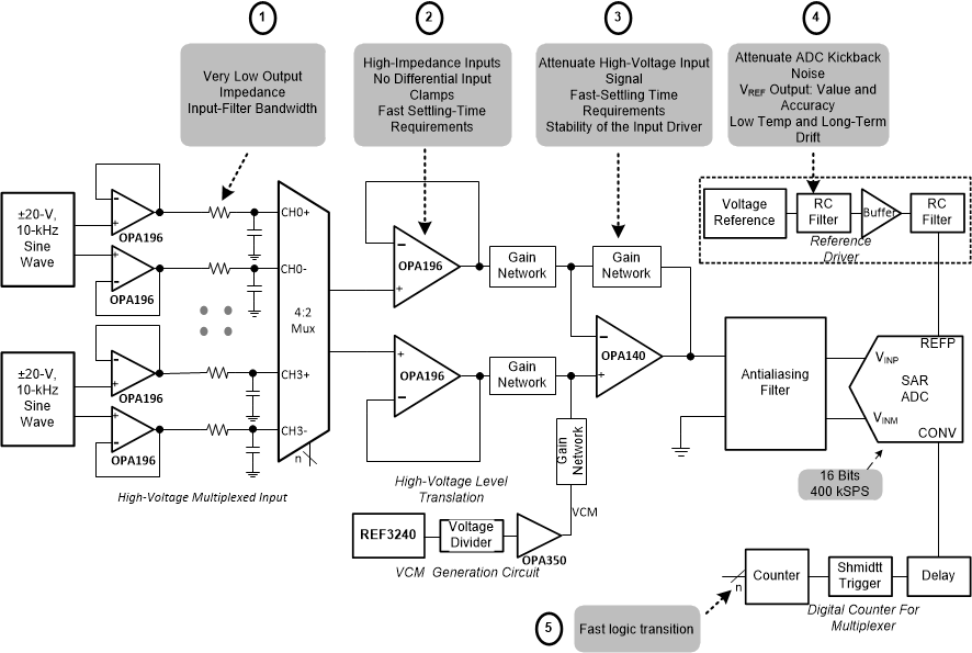
Figure 49 shows a 16-bit, differential, 4-channel, multiplexed, data-acquisition system. This example is typical in industrial applications that require low distortion and a high-voltage differential input. The circuit uses the ADS8864, a 16-bit, 400-kSPS successive-approximation-resistor (SAR), analog-to-digital converter (ADC), along with a precision, high-voltage, signal-conditioning front-end, and a 4-channel differential multiplexer (mux). This application example shows the process for optimizing the precision, high-voltage, front-end drive circuit using the OPA196 and OPA140 to achieve excellent dynamic performance and linearity with the ADS8864. The full TI Precision Design can be found in TIDU181.
 Figure 49. OPA196 in 16-Bit, 400-kSPS, 4-Channel, Multiplexed Data Acquisition System for High-Voltage Inputs With Lowest Distortion
 8.2.2.1 Design Requirements
The primary objective is to design a ±20-V, differential, 4-channel, multiplexed, data acquisition system with lowest distortion using the 16-bit ADS8864 at a throughput of 400 kSPS for a 10-kHz, full-scale, pure sine-wave input. The design requirements for this block design are:
- System supply voltage: ±15 V
- ADC supply voltage: 3.3 V
- ADC sampling rate: 400 kSPS
- ADC reference voltage (REFP): 4.096 V
- System input signal: A high-voltage differential input signal with a peak amplitude of 10 V and frequency (fIN) of 10 kHz are applied to each differential input of the mux.
8.2.2.2 Detailed Design Procedure
The purpose of this application example is to design an optimal, high-voltage, multiplexed, data-acquisition system for highest system linearity and fast settling. The overall system block diagram is shown in Figure 49. The circuit is a multichannel, data-acquisition, signal chain consisting of an input low-pass filter, multiplexer (mux), mux output buffer, attenuating SAR ADC driver, digital counter for the mux, and the reference driver. The architecture allows fast sampling of multiple channels using a single ADC, providing a low-cost solution. The two primary design considerations to maximize the performance of a precision, multiplexed, data-acquisition system are the mux input analog front-end and the high-voltage, level translation, SAR ADC driver design. However, carefully design each analog circuit block based on the ADC performance specifications in order to achieve the fastest settling at 16-bit resolution and lowest distortion system. Figure 49 includes the most important specifications for each individual analog block.
This design systematically approaches each analog circuit block to achieve a 16-bit settling for a full-scale input stage voltage and linearity for a 10-kHz sinusoidal input signal at each input channel. The first step in the design is to understand the requirement for an extremely-low-impedance input-filter design for the mux. This understanding helps in the decision of an appropriate input filter and selection of a mux to meet the system settling requirements. The next important step is the design of the attenuating analog front-end (AFE) used to level translate the high-voltage input signal to a low-voltage ADC input while maintaining the amplifier stability. Then, the next step is to design a digital interface to switch the mux input channels with minimum delay. The final design challenge is to design a high-precision, reference-driver circuit that provides the required REFP reference voltage with low offset, drift, and noise contributions.
 |
For step-by-step design procedure, circuit schematics, bill of materials, PCB files, simulation results, and test results, refer to TI Precision Design TIDU181, 16-bit, 400-kSPS, 4-Channel, Multiplexed Data Acquisition System for High Voltage Inputs with Lowest Distortion. |
8.2.3 Slew Rate Limit for Input Protection
In control systems for valves or motors, abrupt changes in voltages or currents can cause mechanical damages. By controlling the slew rate of the command voltages into the drive circuits, the load voltages ramps up and down at a safe rate. For symmetrical slew-rate applications (positive slew rate equals negative slew rate), one additional op amp provides slew-rate control for a given analog gain stage. The unique input protection and high output current and slew rate of the OPAx196 make the device an optimal amplifier to achieve slew rate control for both dual- and single-supply systems.Figure 50 shows the OPA196 in a slew-rate limit design.
 Figure 50. Slew Rate Limiter Uses One Op Amp
 |
For step-by-step design procedure, circuit schematics, bill of materials, PCB files, simulation results, and test results, refer to TI Precision Design TIDU026, Slew Rate Limiter Uses One Op Amp. |