SBOSA11E March   2020  – December 2023 OPA206 , OPA2206 , OPA4206

PRODUCTION DATA  

  1.   1
  2. Features
  3. Applications
  4. Description
  5. Pin Configuration and Functions
  6. Specifications
    1. 5.1 Absolute Maximum Ratings
    2. 5.2 ESD Ratings
    3. 5.3 Recommended Operating Conditions
    4. 5.4 Thermal Information: OPA206
    5. 5.5 Thermal Information: OPA2206
    6. 5.6 Thermal Information: OPA4206
    7. 5.7 Electrical Characteristics: VS = ±5 V
    8. 5.8 Electrical Characteristics: VS = ±15 V
    9. 5.9 Typical Characteristics
  7. Parameter Measurement Information
    1. 6.1 Typical Specifications and Distributions
  8. Detailed Description
    1. 7.1 Overview
    2. 7.2 Functional Block Diagram
    3. 7.3 Feature Description
      1. 7.3.1 Input Overvoltage Protection
      2. 7.3.2 Input Offset Trimming
      3. 7.3.3 Lower Input Bias With Super-Beta Inputs
      4. 7.3.4 Overload Power Limiter
      5. 7.3.5 EMI Rejection
    4. 7.4 Device Functional Modes
  9. Application and Implementation
    1. 8.1 Application Information
    2. 8.2 Typical Applications
      1. 8.2.1 Voltage Attenuator
        1. 8.2.1.1 Design Requirements
        2. 8.2.1.2 Detailed Design Procedure
        3. 8.2.1.3 Application Curves
      2. 8.2.2 Discrete, Two-Op-Amp Instrumentation Amplifier
      3. 8.2.3 Input Buffer and Protection for ADC Driver
    3. 8.3 Power Supply Recommendations
    4. 8.4 Layout
      1. 8.4.1 Layout Guidelines
      2. 8.4.2 Layout Example
  10. Device and Documentation Support
    1. 9.1 Device Support
      1. 9.1.1 Development Support
        1. 9.1.1.1 PSpice® for TI
    2. 9.2 Documentation Support
      1. 9.2.1 Related Documentation
    3. 9.3 Receiving Notification of Documentation Updates
    4. 9.4 Support Resources
    5. 9.5 Trademarks
    6. 9.6 Electrostatic Discharge Caution
    7. 9.7 Glossary
  11. 10Revision History
  12. 11Mechanical, Packaging, and Orderable Information

Package Options

Refer to the PDF data sheet for device specific package drawings

Mechanical Data (Package|Pins)
  • D|8
Thermal pad, mechanical data (Package|Pins)
Orderable Information

Typical Characteristics

at TA = 25°C, VS = ±15 V, VCM = VOUT = mid-supply, and RL = 10 kΩ (unless otherwise noted)

Table 5-1 Table of Graphs
DESCRIPTION FIGURE
Offset Voltage Production Distribution at 25°C Figure 5-1
Offset Voltage Distribution at 125°C Figure 5-2
Offset Voltage Distribution at –40°C Figure 5-3
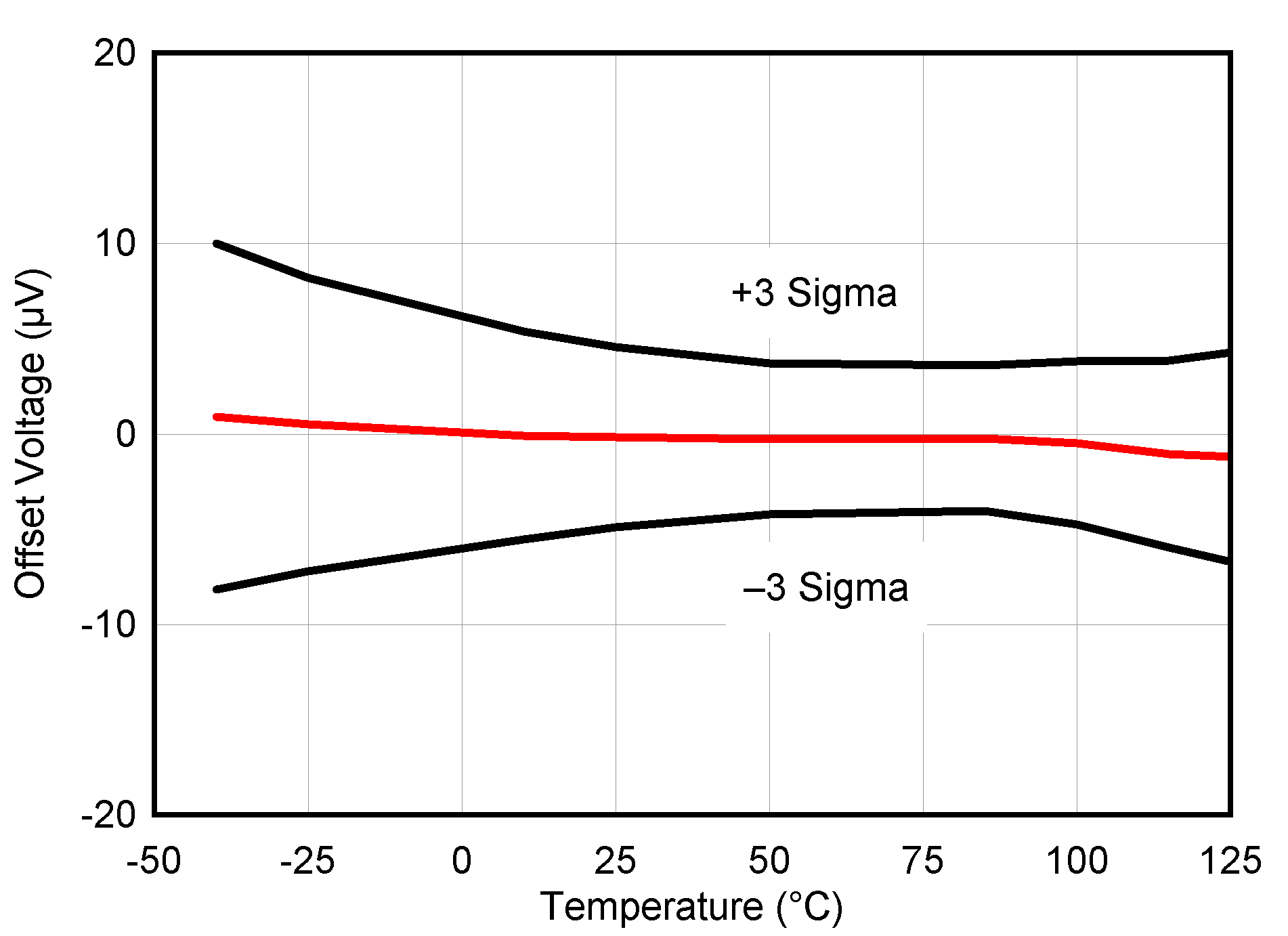
Offset Voltage vs Temperature Figure 5-4
Offset Voltage Drift Production Distribution Figure 5-5
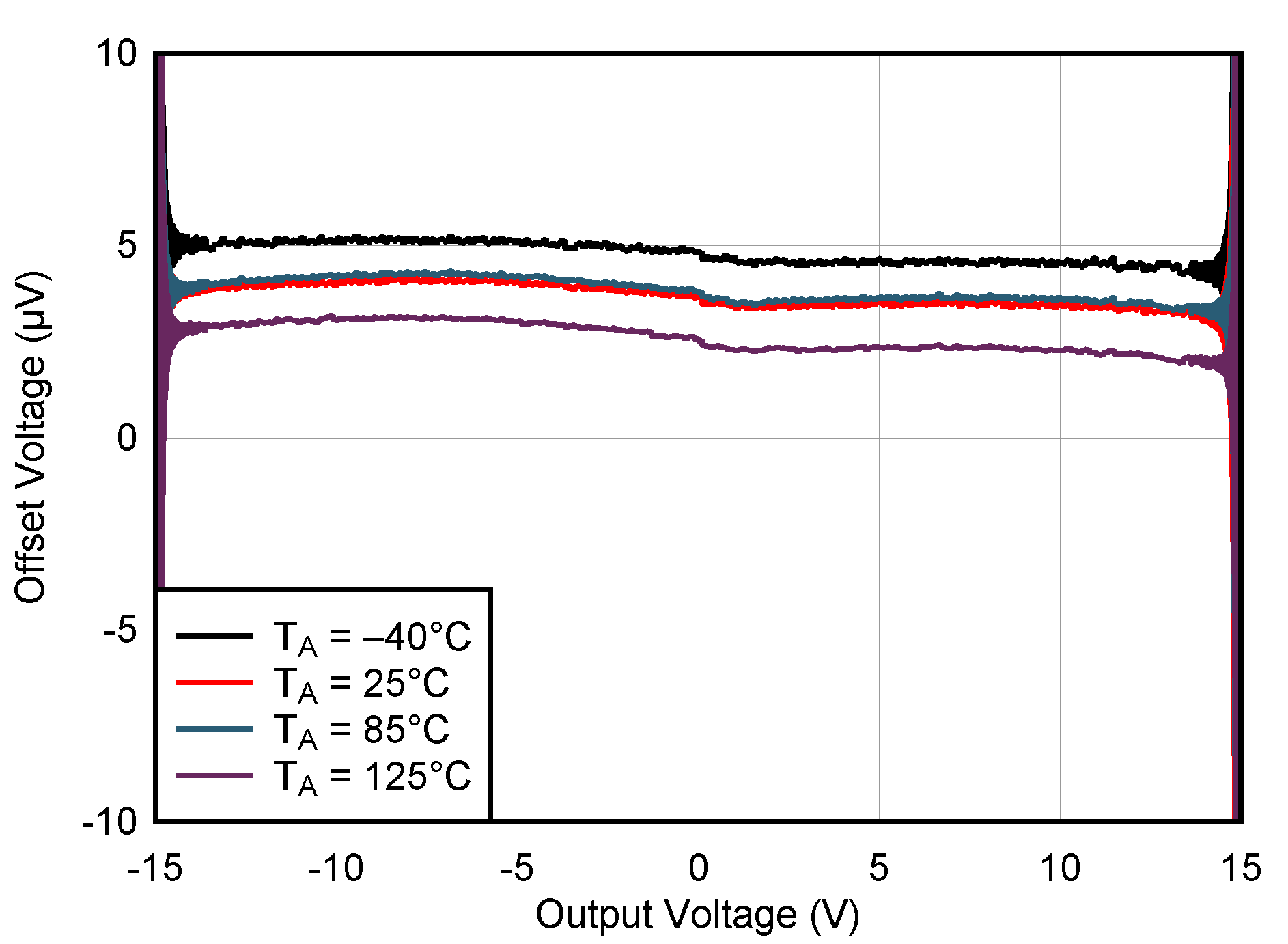
Offset Voltage vs Output Voltage Figure 5-6
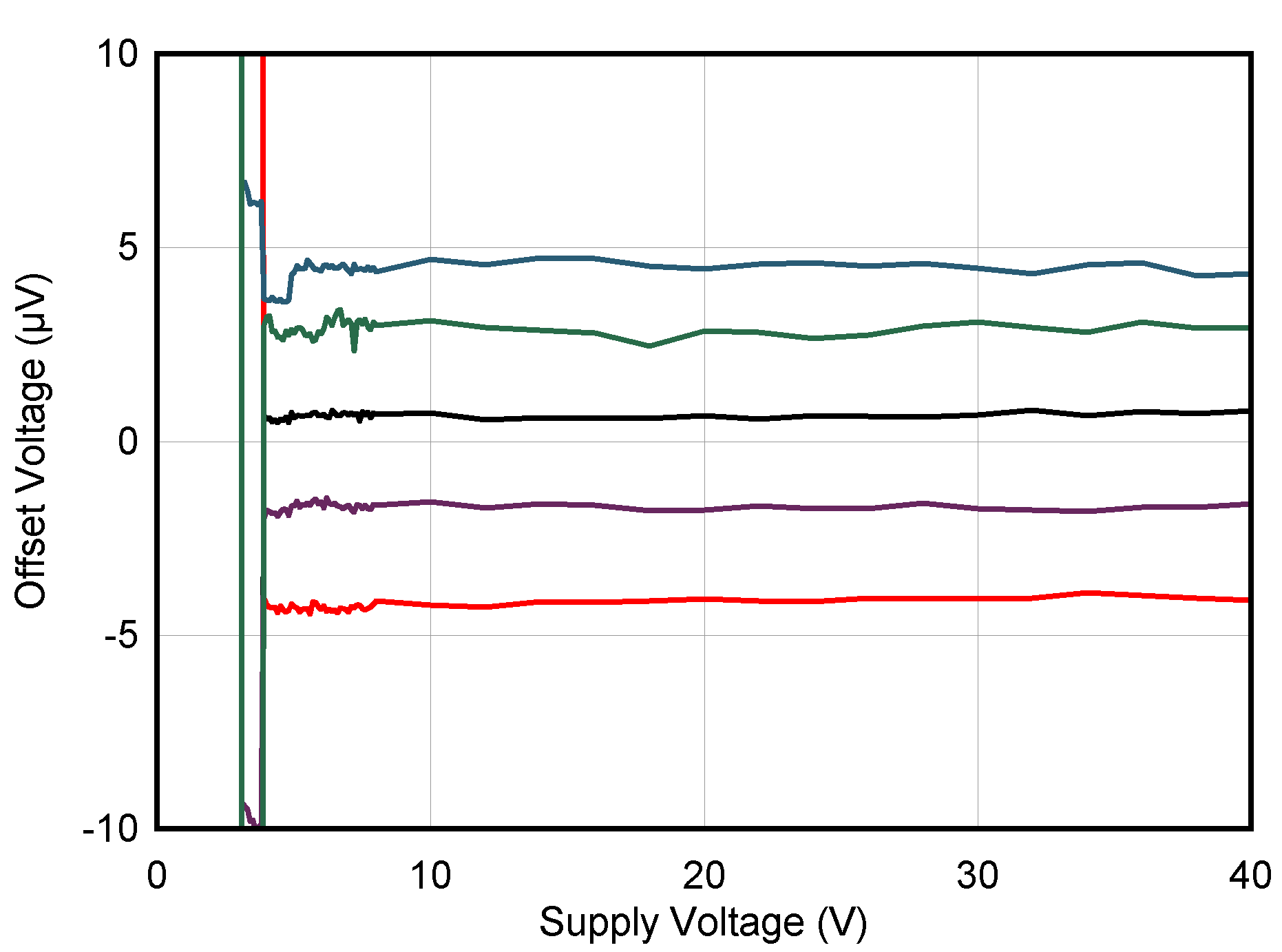
Offset Voltage vs Power Supply Voltage Figure 5-7
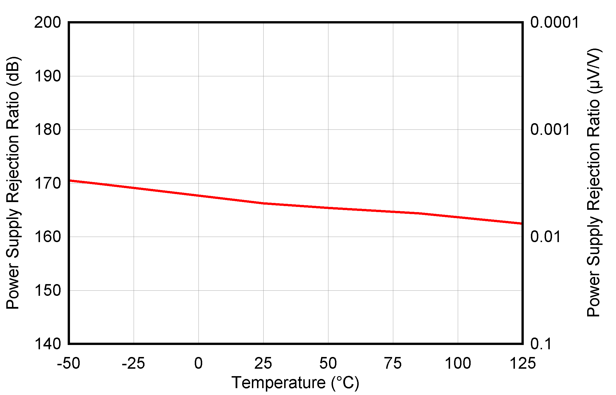
Power-Supply Rejection Ratio vs Temperature Figure 5-8
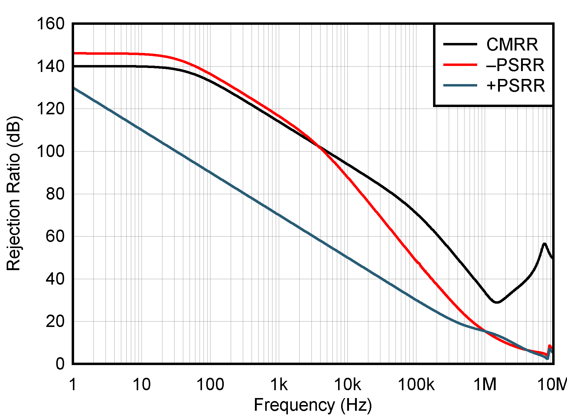
Power-Supply and Common-Mode Rejection Ratio vs Frequency Figure 5-9
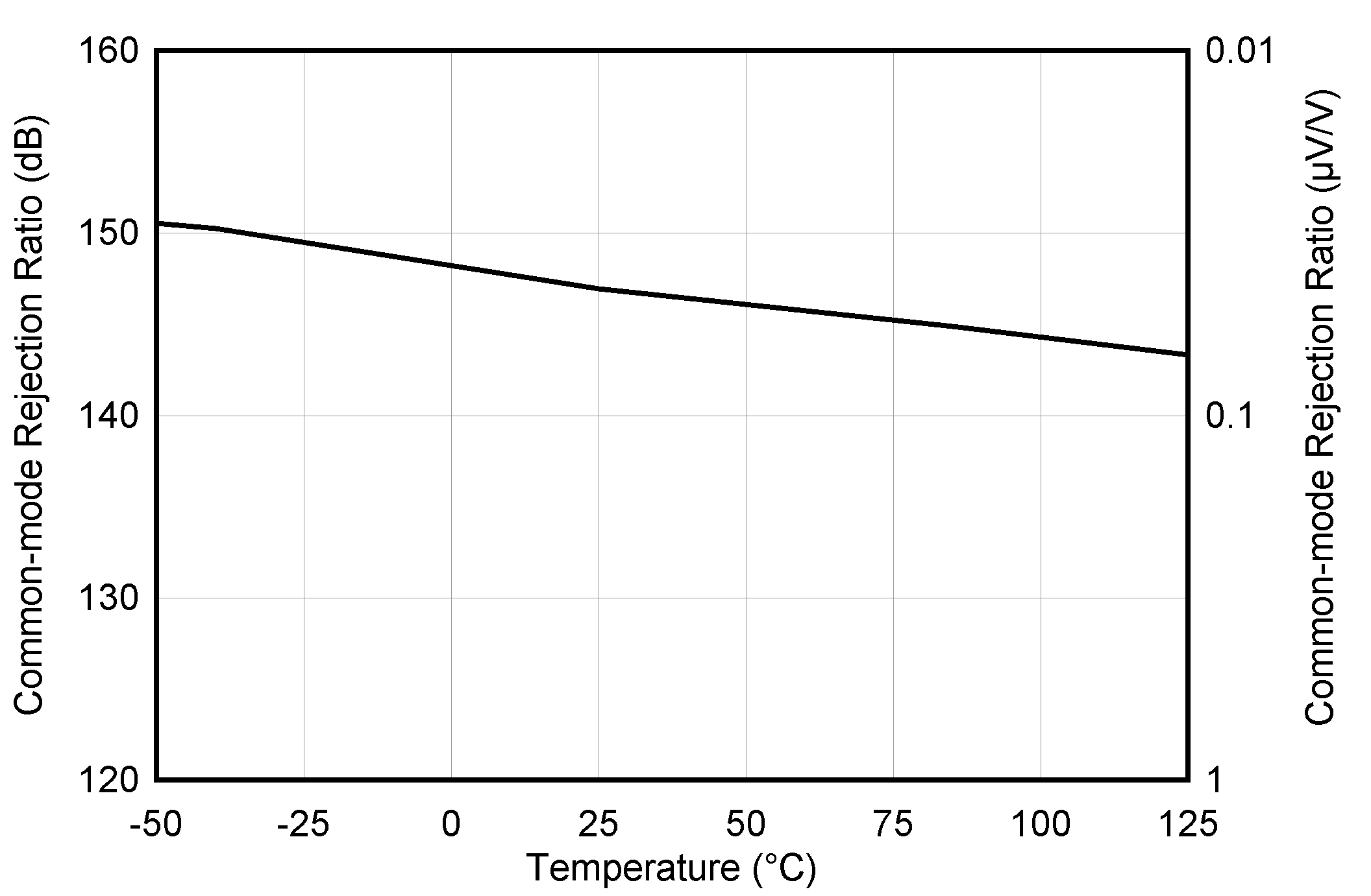
Common-Mode Rejection Ratio vs Temperature Figure 5-10
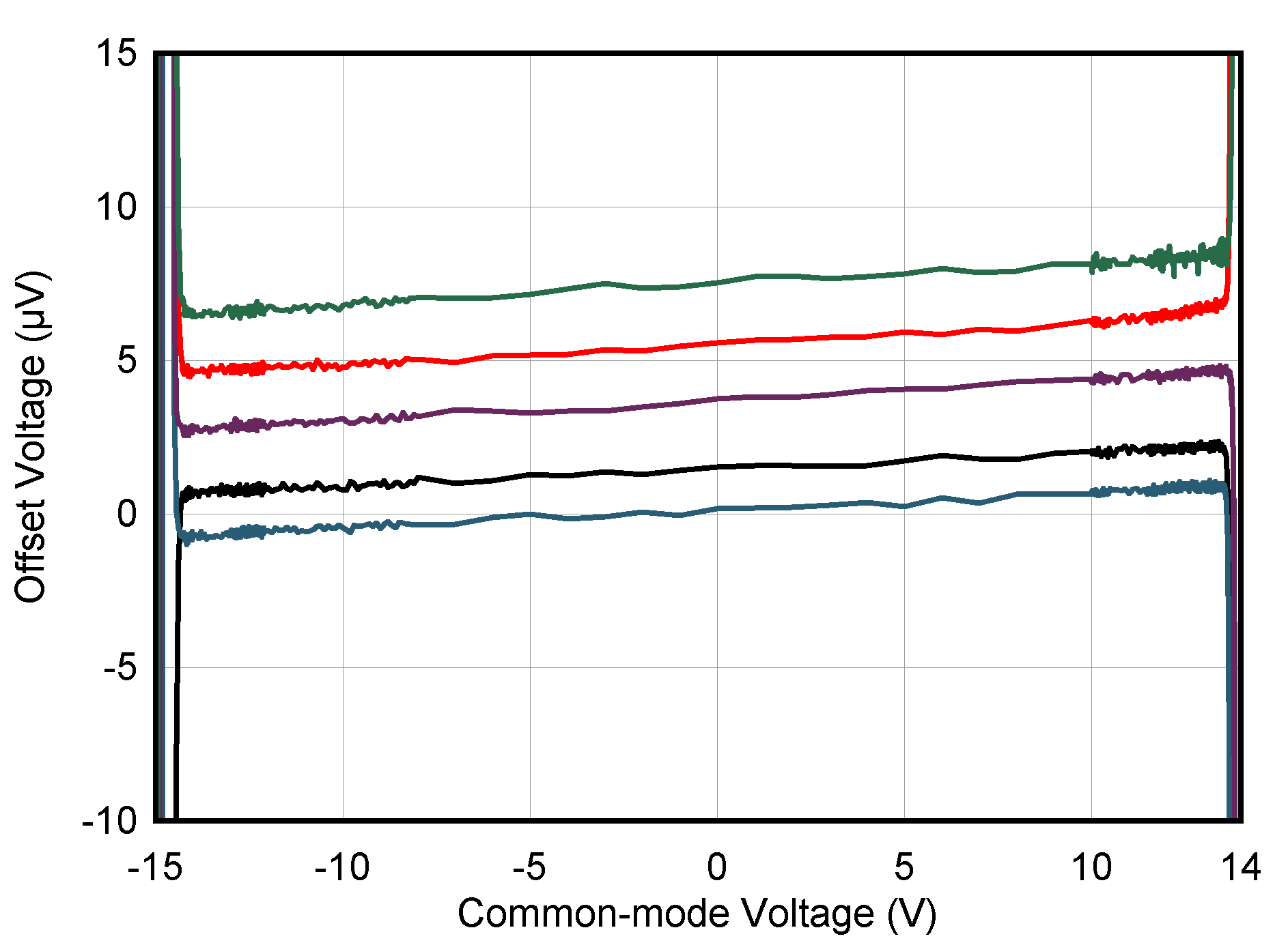
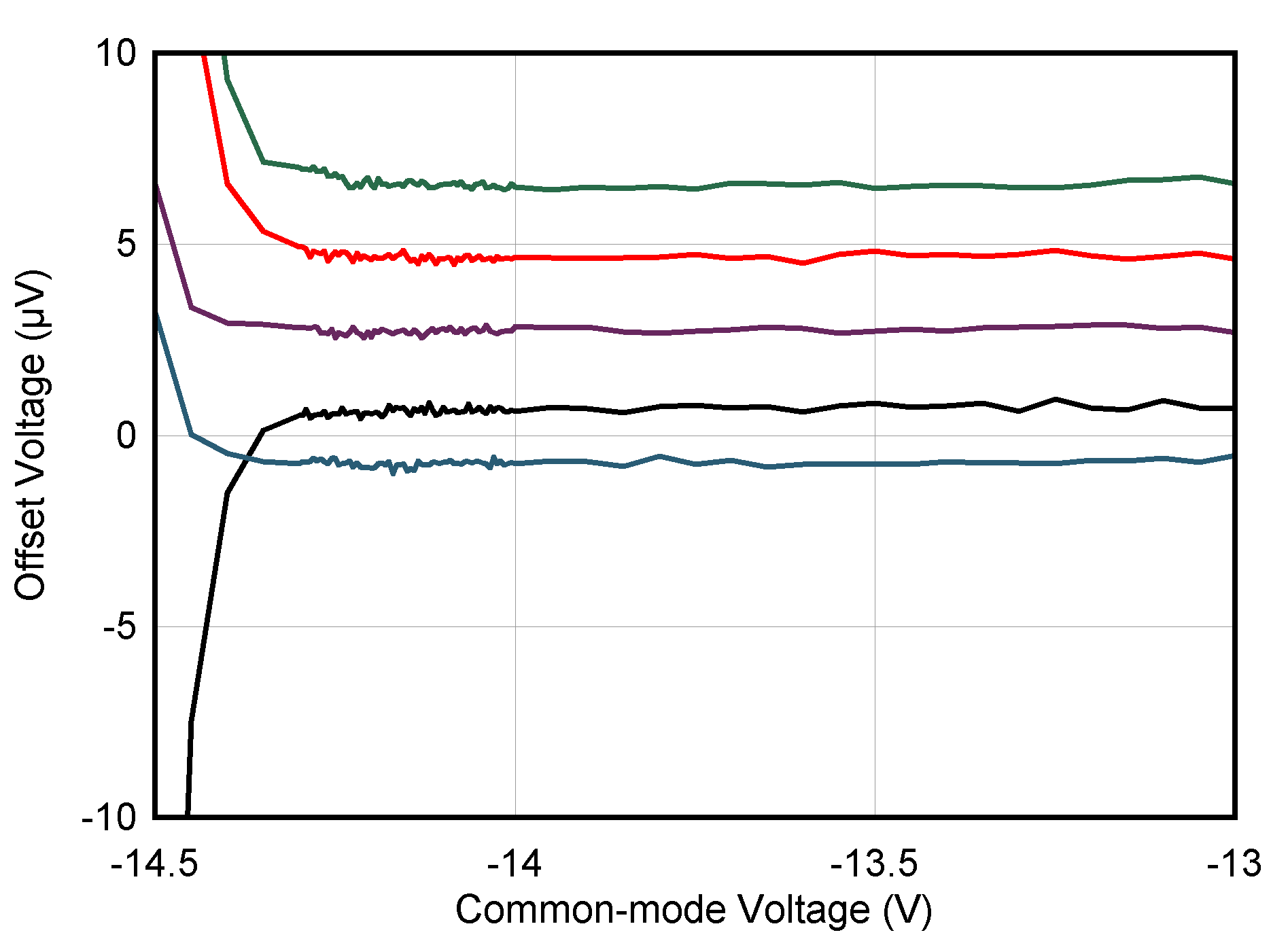
Offset Voltage vs Common-Mode Voltage Figure 5-11
Offset Voltage vs VCM at Low Supply Figure 5-12
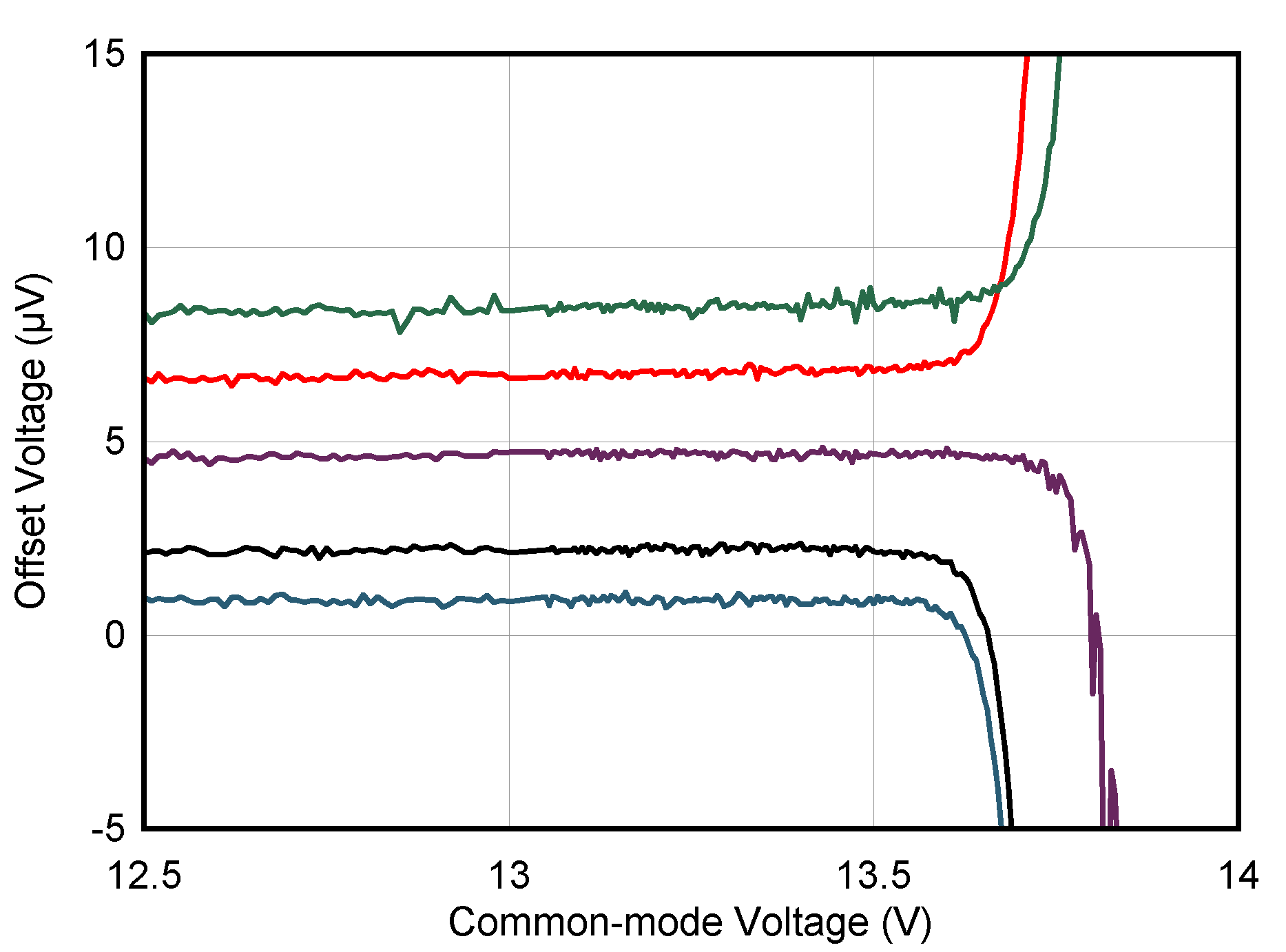
Offset Voltage vs VCM at High Supply Figure 5-13
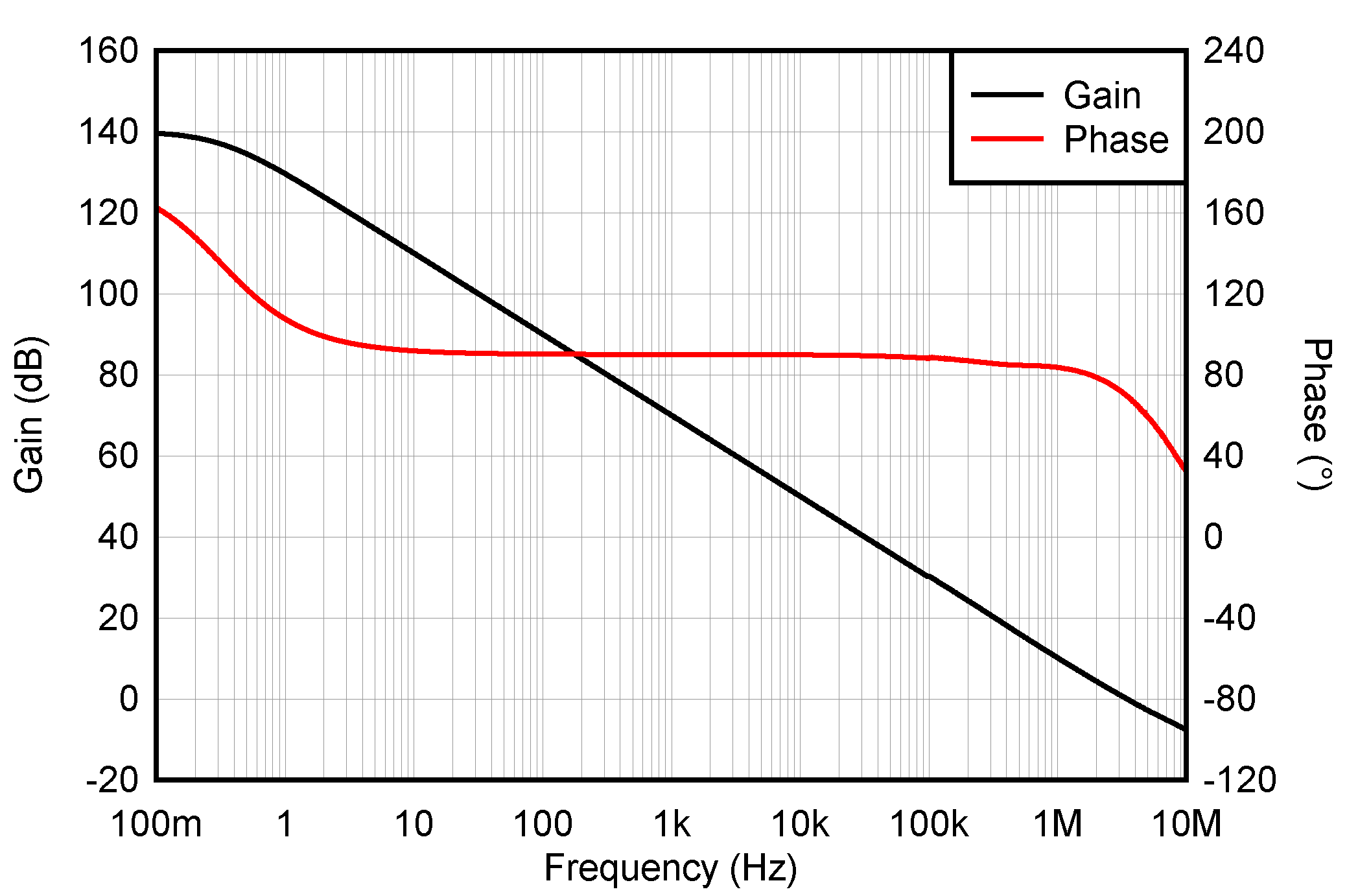
Open-Loop Gain and Phase vs Frequency Figure 5-14
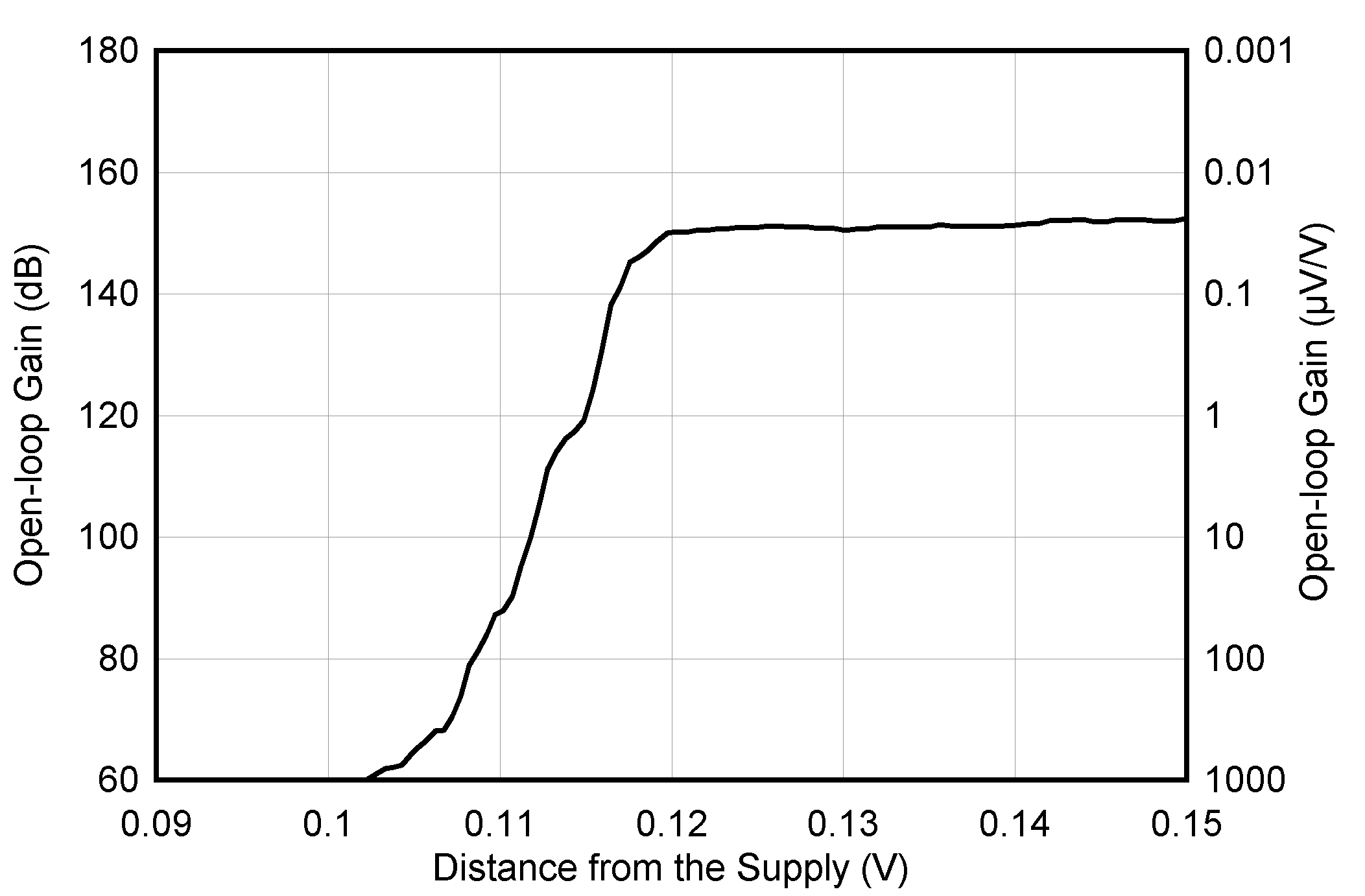
Open-Loop Gain vs Distance From Supply Figure 5-15
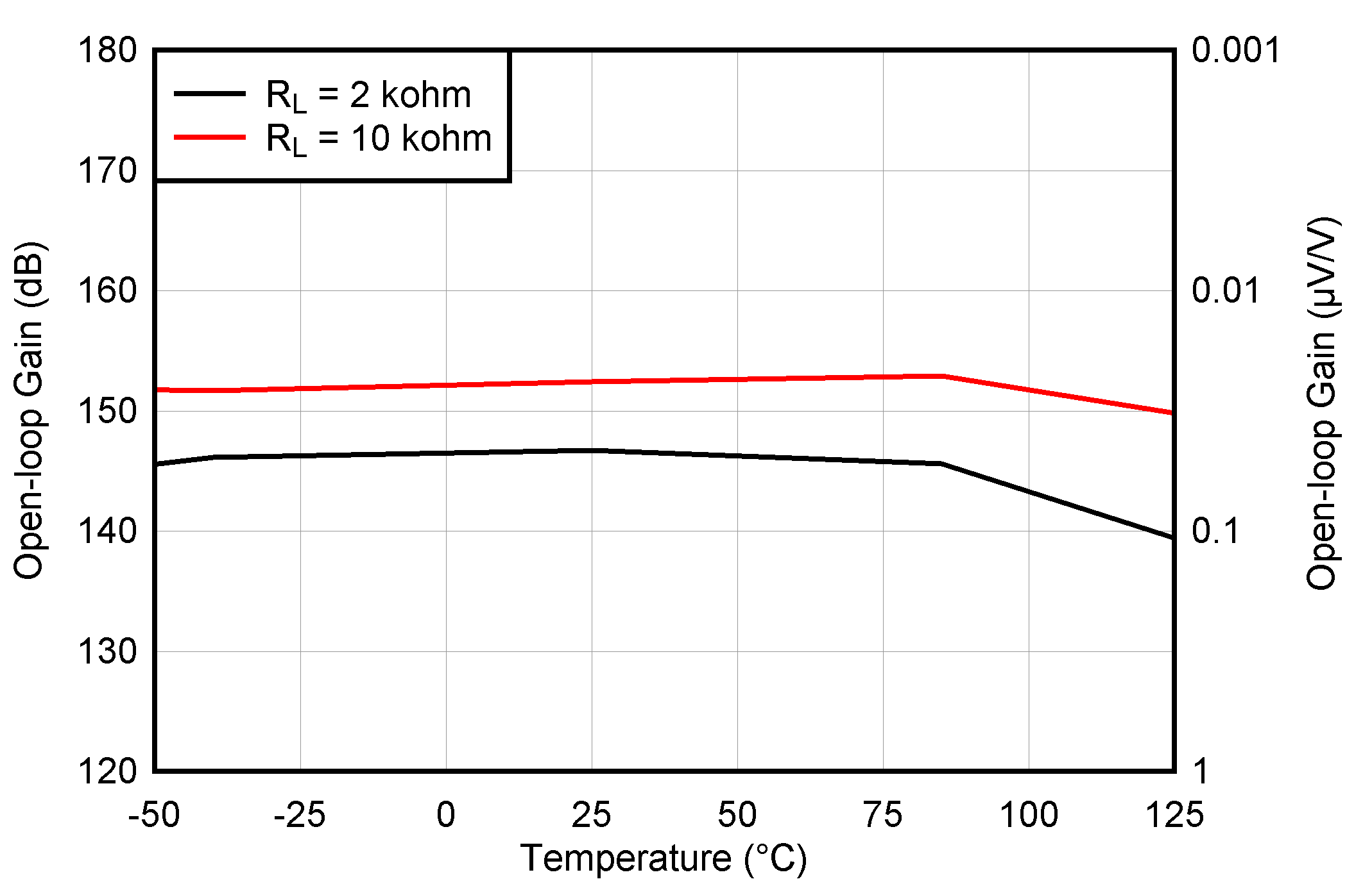
Open-Loop Gain vs Temperature Figure 5-16
Closed-Loop Gain vs Frequency Figure 5-17
Input Bias Production Distribution Figure 5-18
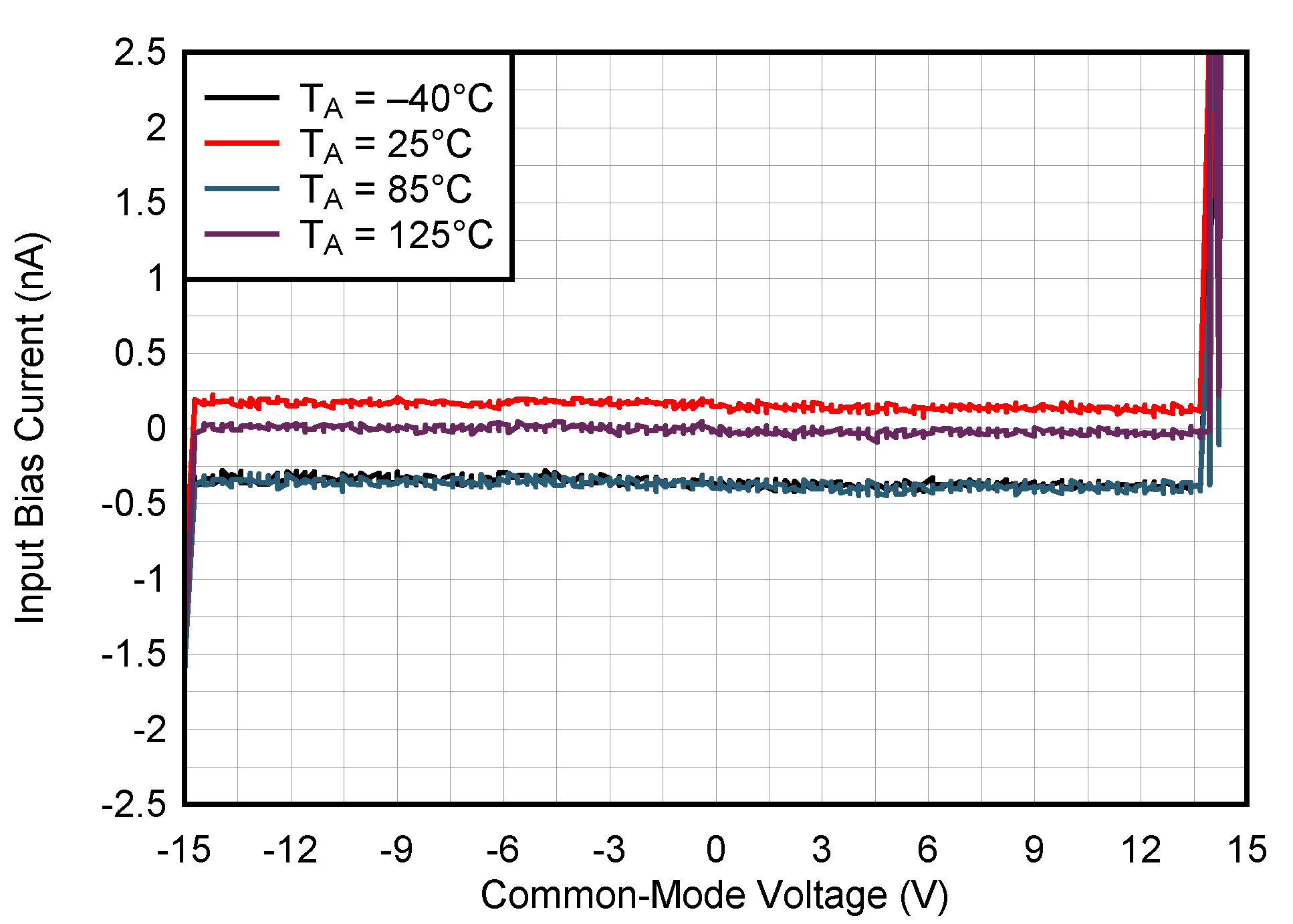
Input Bias vs Common-Mode Voltage Figure 5-19
Input Bias and Input Offset Current vs Temperature Figure 5-20
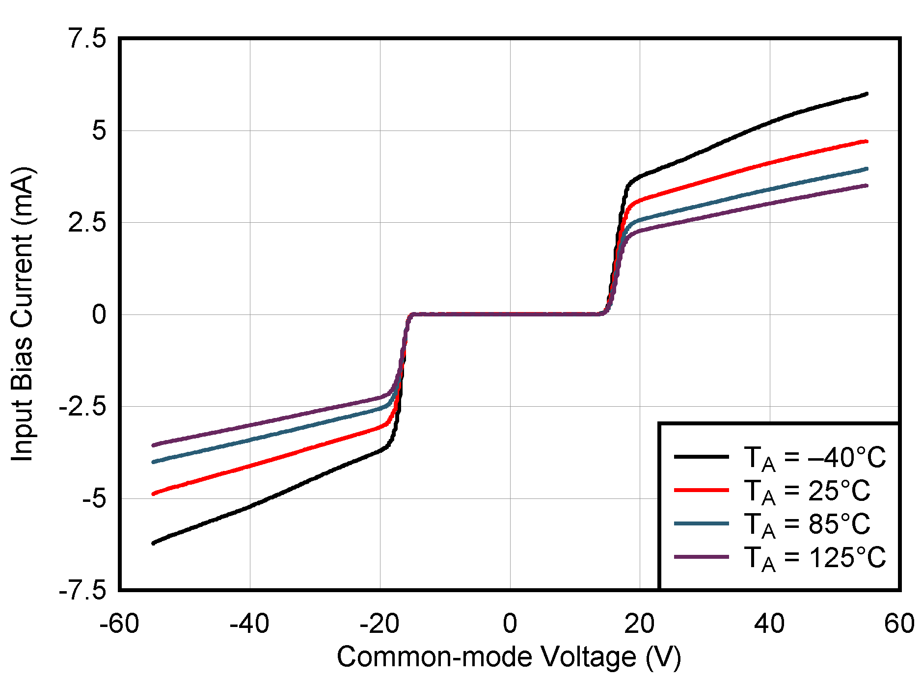
Input Bias vs. Overvoltage-Protected Common-Mode Range Figure 5-21
Input Offset Current Production Distribution Figure 5-22
Voltage Noise Density vs Frequency Figure 5-23
0.1-Hz to 10-Hz Noise Figure 5-24
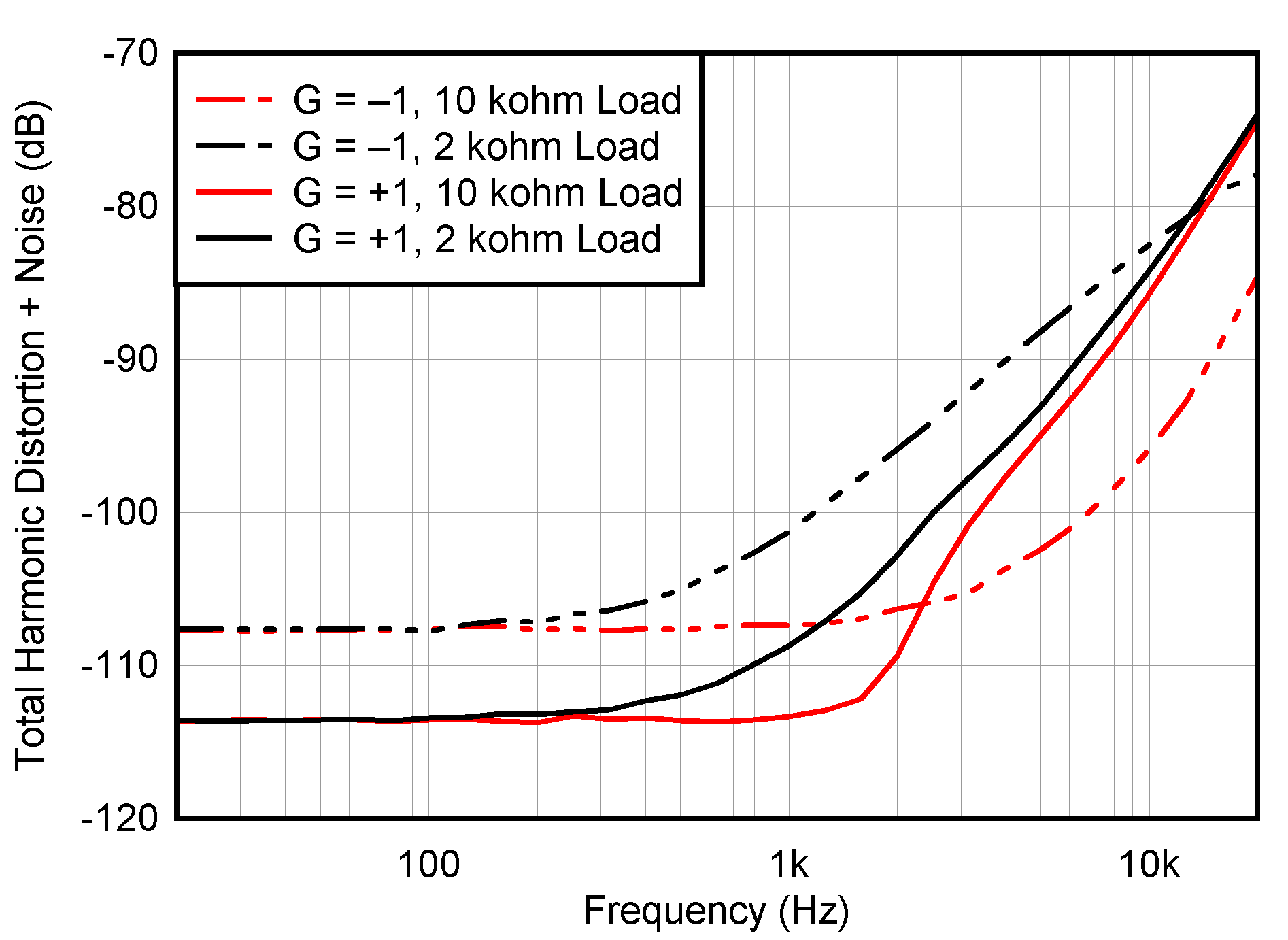
Total Harmonic Distortion + Noise Ratio vs Frequency Figure 5-25
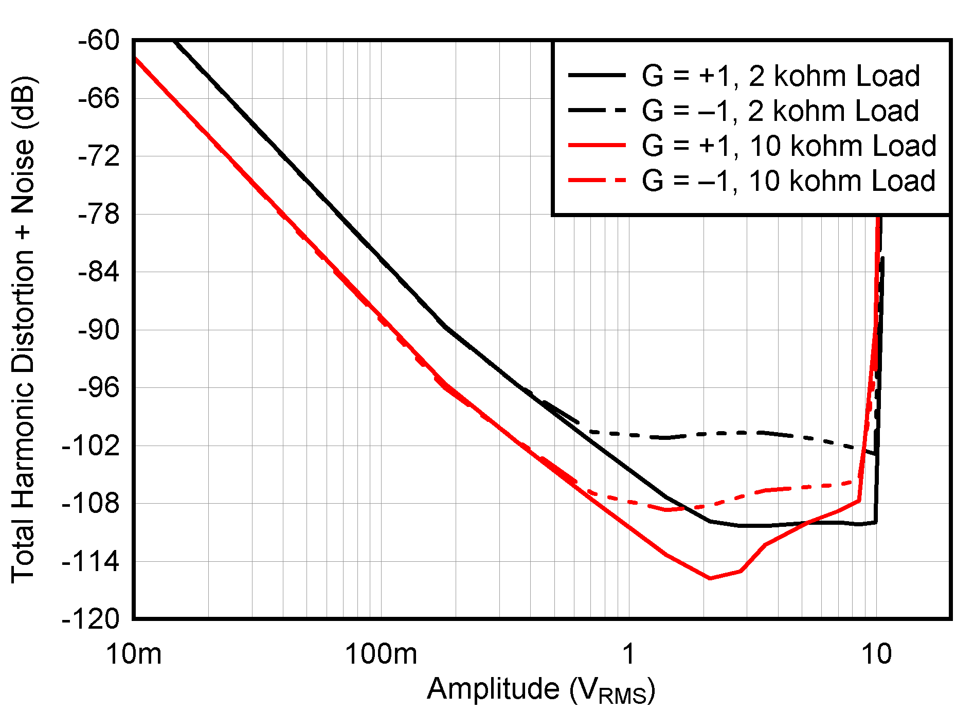
Total Harmonic Distortion + Noise Ratio vs Output Amplitude Figure 5-26
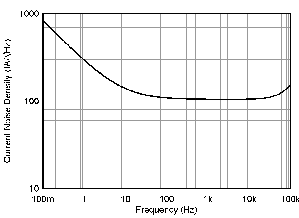
Current Noise vs Frequency Figure 5-27
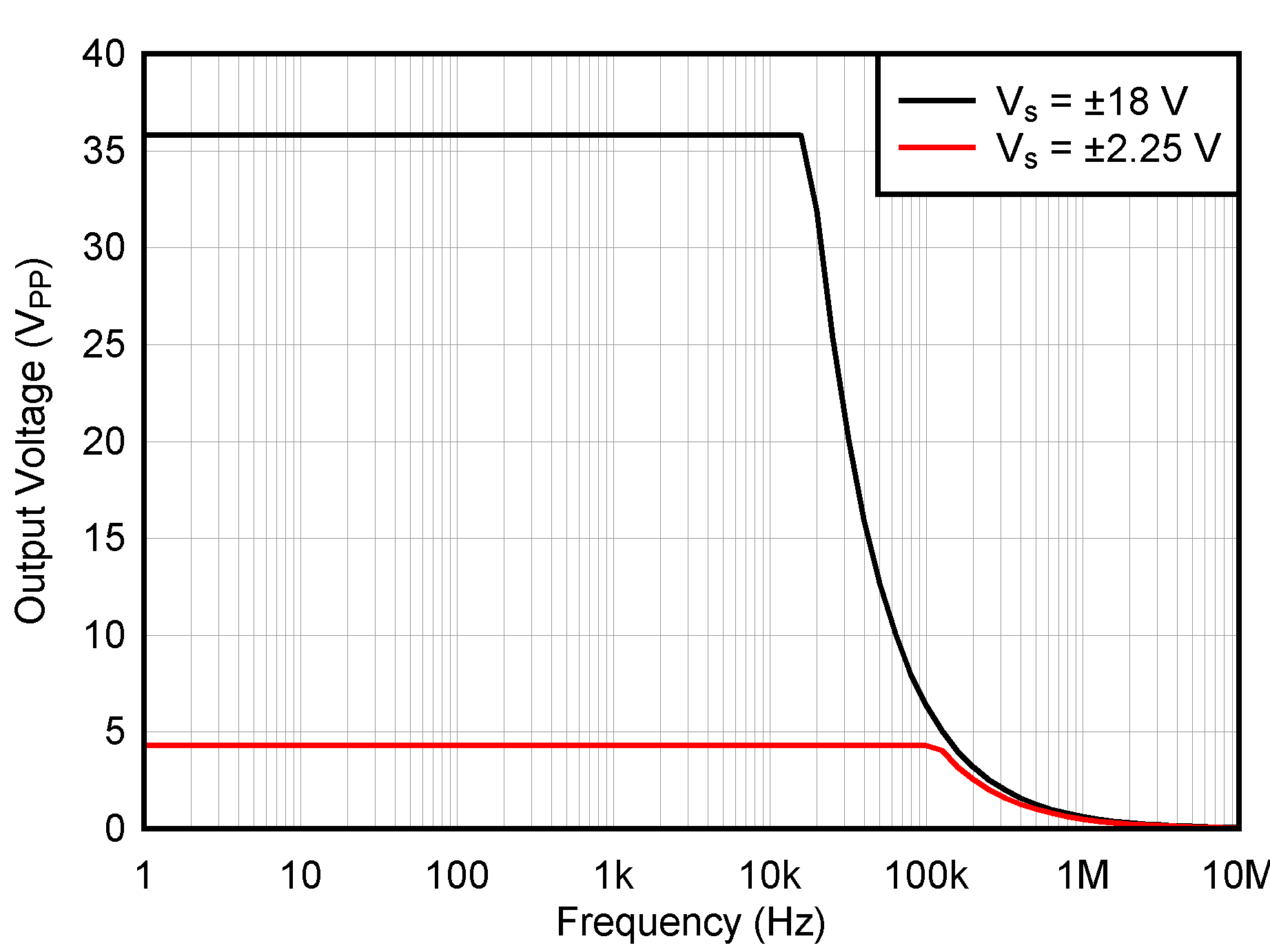
Maximum Output Voltage vs Frequency Figure 5-28
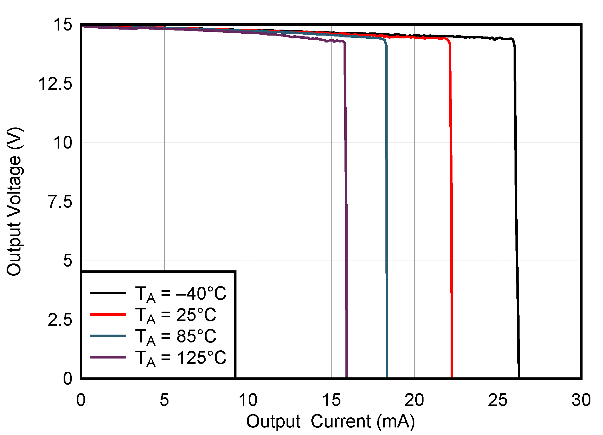
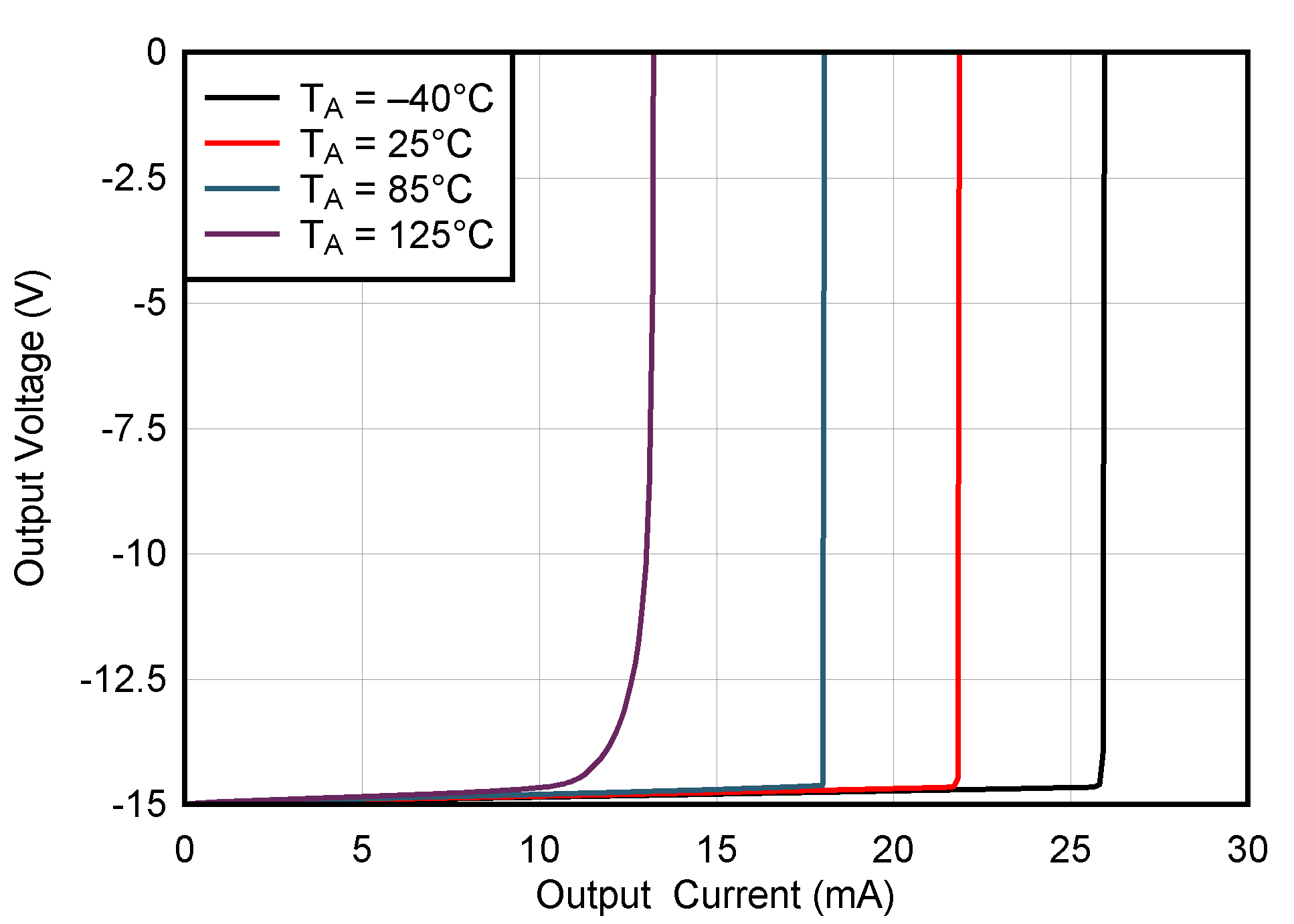
Output Voltage Swing vs Output Sourcing Current Figure 5-29
Output Voltage Swing vs Output Sinking Current Figure 5-30
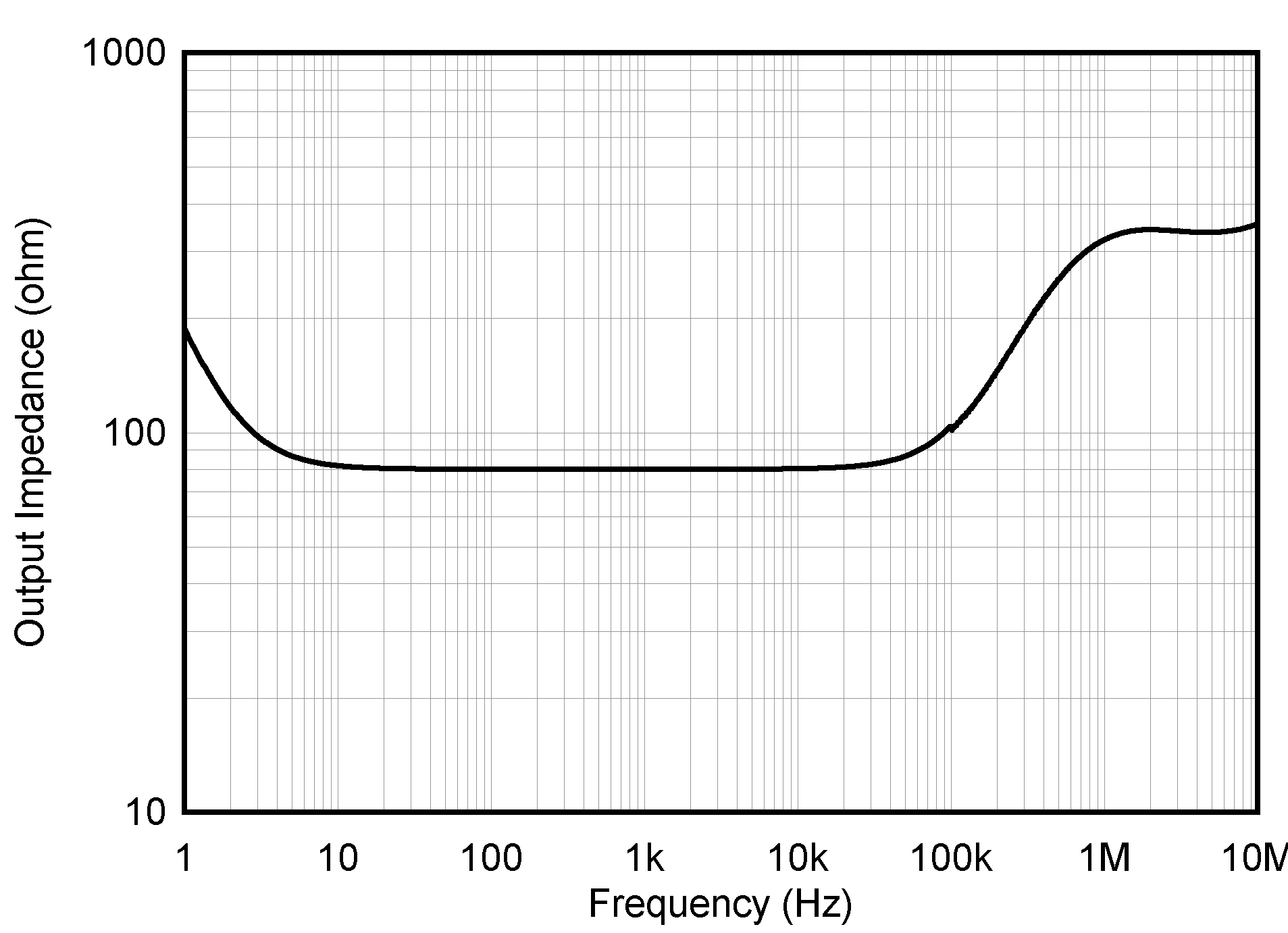
Open-Loop Output Impedance vs Frequency Figure 5-31
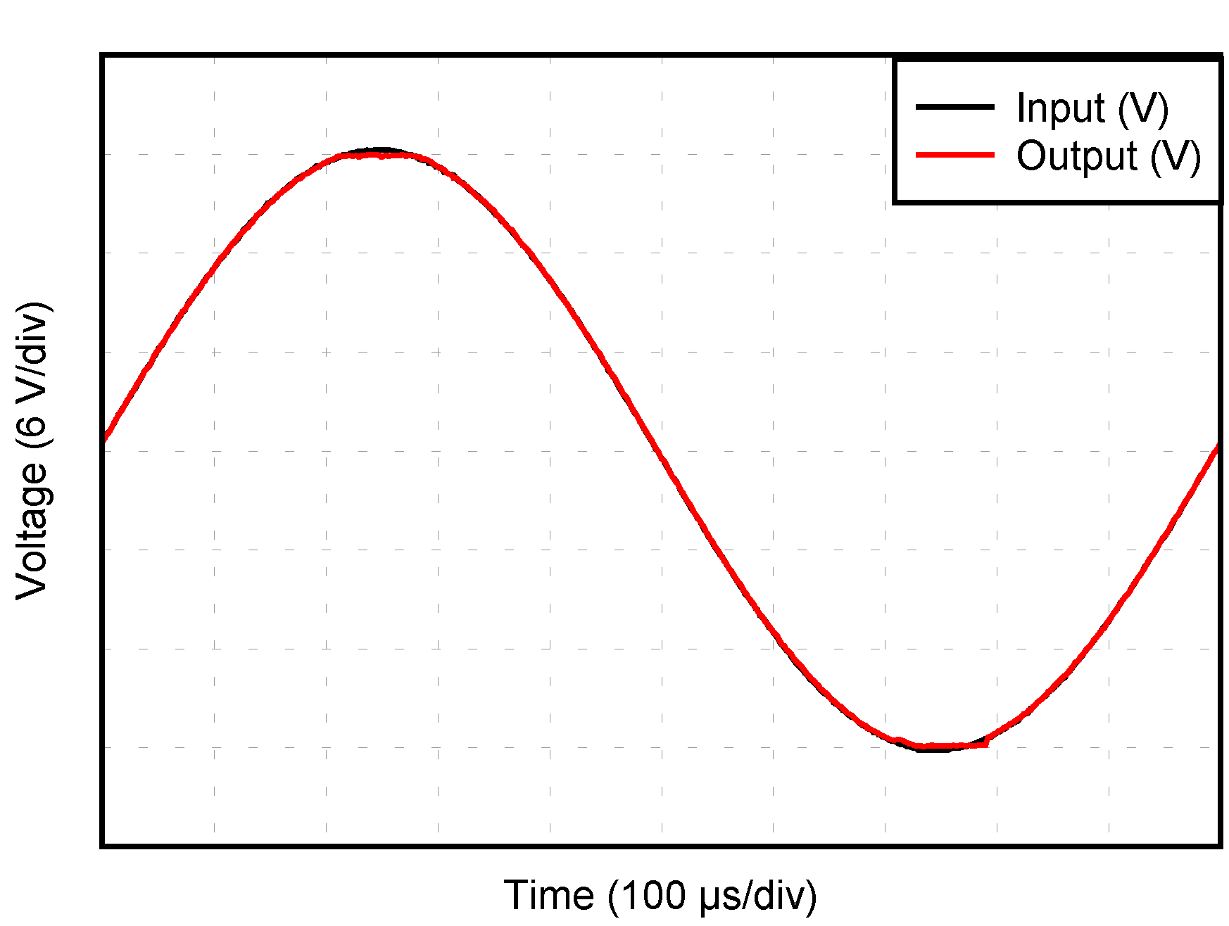
No Phase Reversal Figure 5-32
Small-Signal Overshoot vs Capacitive Load, Gain = 1 Figure 5-33
Small-Signal Overshoot vs Capacitive Load, Gain = –1 Figure 5-34
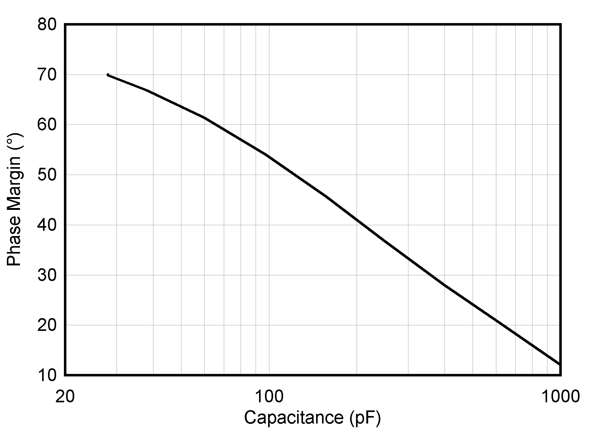
Phase Margin vs Capacitive Load Figure 5-35
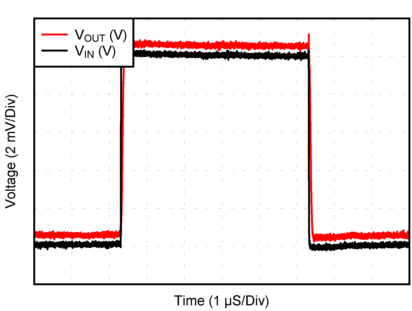
Positive Overload Recovery, Gain = –1 Figure 5-36
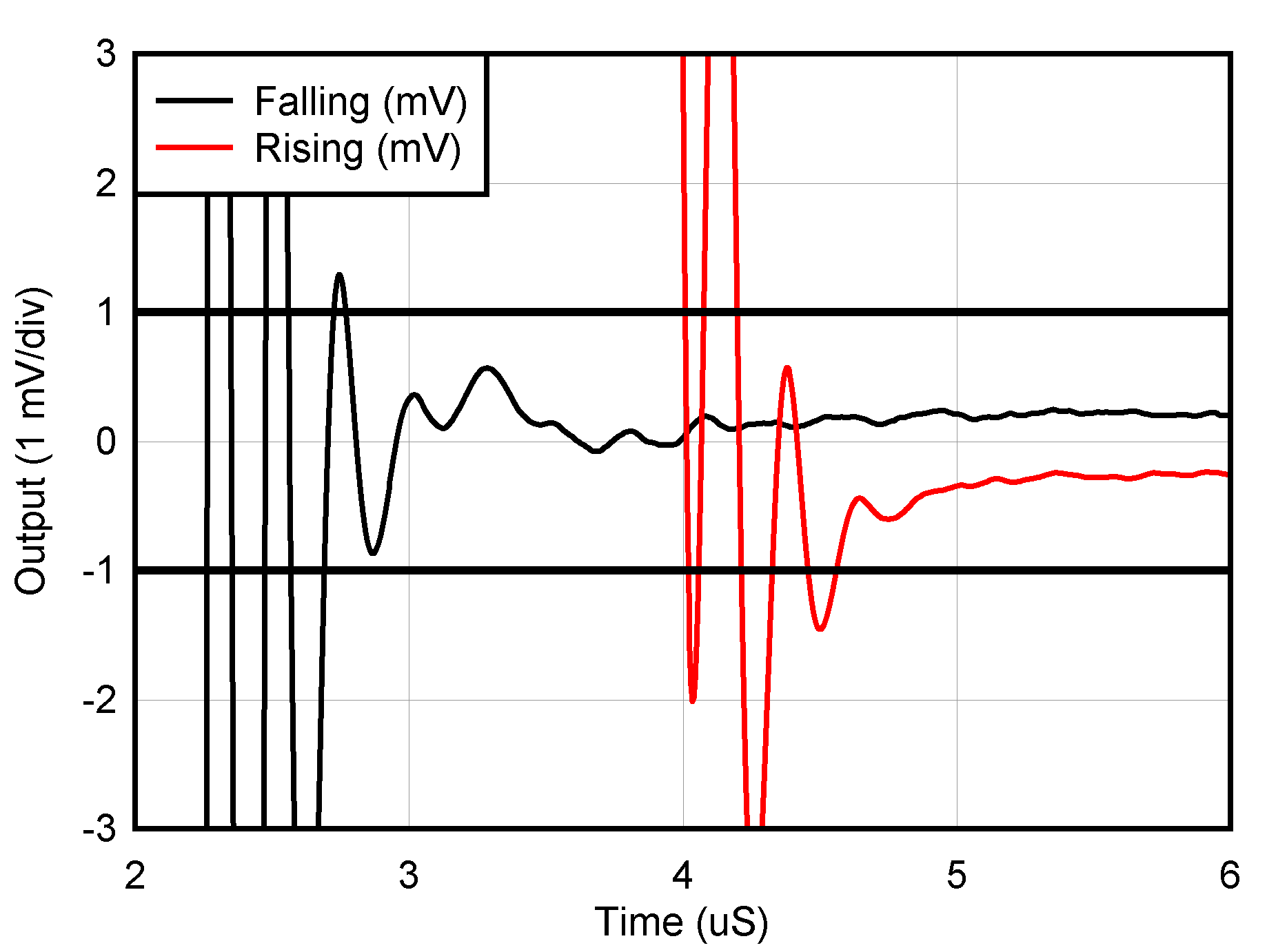
Negative Overload Recovery, Gain = –1 Figure 5-37
Settling Time Figure 5-38
Small-Signal Step Response, Gain = 1 Figure 5-39
Small-Signal Step Response, Gain = –1 Figure 5-40
Large-Signal Step Response, Gain = 1 Figure 5-41
Large-Signal Step Response, Gain = –1 Figure 5-42
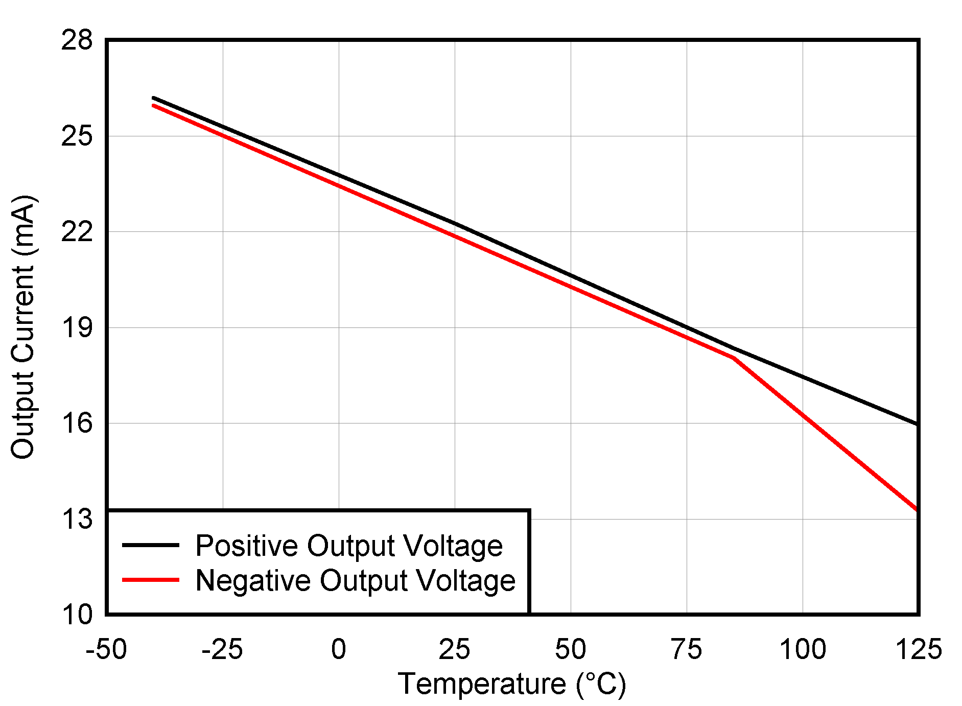
Short-Circuit Current vs Temperature Figure 5-43
Electromagnetic Interference Rejection (EMIRR) Figure 5-44
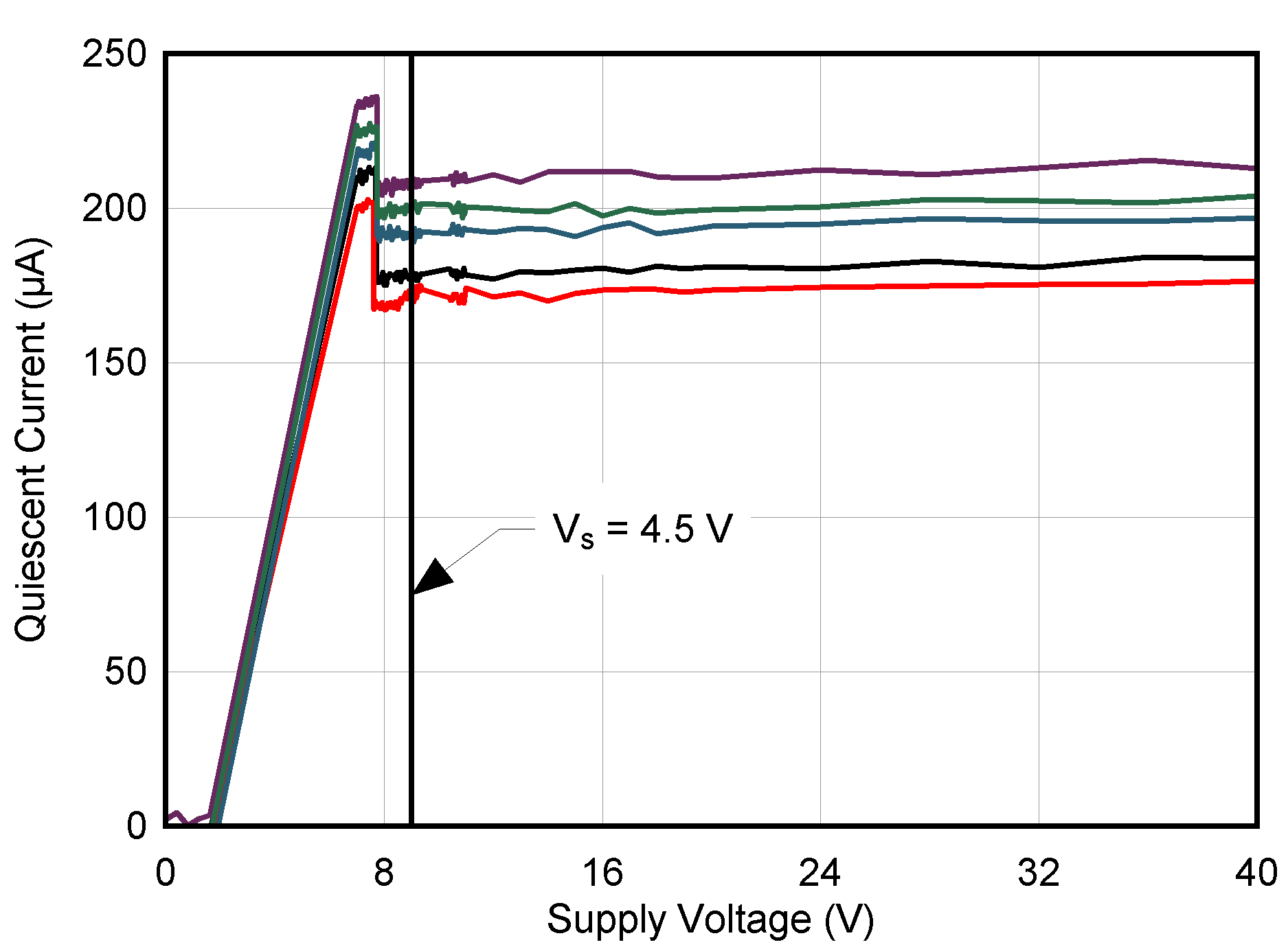
Quiescent Current vs Supply Voltage Figure 5-45
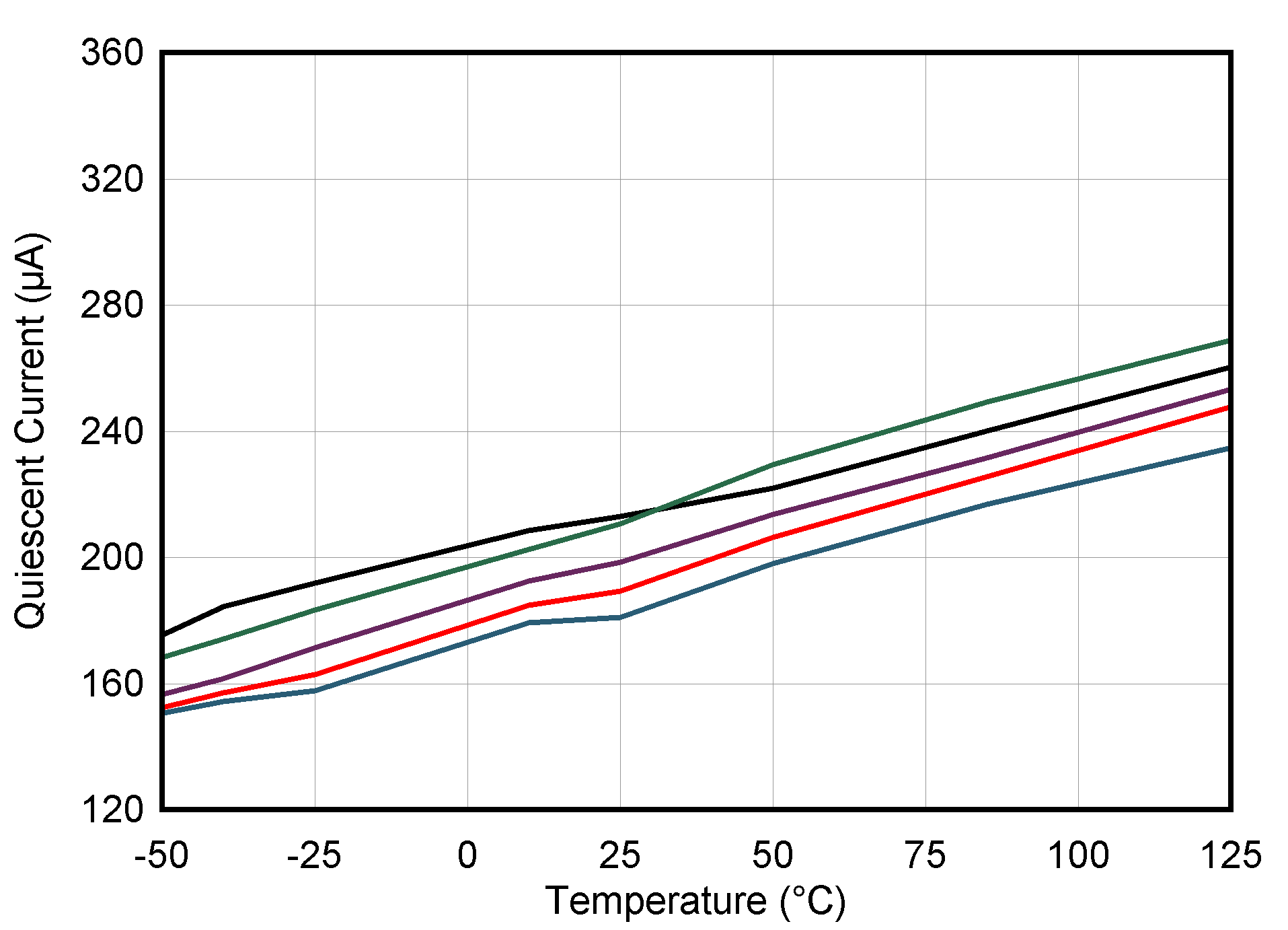
Quiescent Current vs Temperature Figure 5-46
GUID-20230321-SS0I-1ZPR-R6ZT-MQFHPNFZ2GQ6-low.svg
TA = 25°C
Figure 5-1 Offset Voltage Production Distribution
GUID-20230321-SS0I-FCD6-RXFX-B1FJ5SRZQQ0Z-low.svg
TA = –40°C
Figure 5-3 Offset Voltage Distribution
GUID-20230320-SS0I-WF5Q-HSF9-7QB2HK1FQPVW-low.svg
 
Figure 5-5 Offset Voltage Drift Production Distribution
GUID-20210322-CA0I-S308-LTMD-XJPBSDDC3FMZ-low.png
 
Figure 5-7 Offset Voltage vs Power Supply Voltage
GUID-20210322-CA0I-CZLM-LZ3D-KP4GKRQR9LLP-low.png
 
Figure 5-9 Power-Supply and Common-Mode Rejection Ratio vs Frequency
GUID-20210322-CA0I-5XN2-BWNN-Q9WGNHTBZ4T0-low.png
 
Figure 5-11 Offset Voltage vs Common-Mode Voltage
GUID-20210322-CA0I-HXLH-VFZK-PW2TDQK8JNCZ-low.png
 
Figure 5-13 Offset Voltage vs VCM at High Supply
GUID-20210322-CA0I-PMWR-VG7W-ZNQW6WCRN0M2-low.png
 
Figure 5-15 Open-Loop Gain vs Distance From Supply
GUID-20210322-CA0I-RDJN-DHVG-ZZBLPJBPCFRD-low.svg
 
Figure 5-17 Closed-Loop Gain vs Frequency
GUID-20210322-CA0I-5KB1-TMH2-GSPLHGNXRXKT-low.png
 
Figure 5-19 Input Bias vs Common-Mode Voltage
GUID-20210322-CA0I-C8GX-NJWV-WC2NLQHMN21L-low.png
 
Figure 5-21 Input Bias vs Overvoltage-Protected Common-Mode Range
GUID-20210322-CA0I-GZFC-ZJNQ-NQHF0DWX6RT9-low.svg
 
Figure 5-23 Voltage Noise Density vs Frequency
GUID-20210322-CA0I-GR4W-WZCF-3BP0RWBSJFCX-low.png
 
Figure 5-25 Total Harmonic Distortion + Noise Ratio vs Frequency
GUID-20210322-CA0I-KVW6-L6NJ-ZC6ZSSNW6KL5-low.png
 
Figure 5-27 Current Noise vs Frequency
GUID-20210322-CA0I-2CJW-MVXP-K1QGDZDFSQ4V-low.png
 
Figure 5-29 Output Voltage Swing vs Output Sourcing Current
GUID-20210322-CA0I-WNPD-H1BX-MKMR9SHTP5LX-low.png
 
Figure 5-31 Open-Loop Output Impedance vs Frequency
GUID-20210322-CA0I-XTFJ-0BH4-BZFMBPXPR6FR-low.svg
  Gain = 1
Figure 5-33 Small-Signal Overshoot vs Capacitive Load
GUID-20210322-CA0I-SPQB-5NQD-PVTZGF1B6NNN-low.png
 
Figure 5-35 Phase Margin vs Capacitive Load
GUID-20210322-CA0I-FZXK-ZQKL-9V9PSGLJJHB2-low.svg
  Gain = –1
Figure 5-37 Negative Overload Recovery
GUID-20210322-CA0I-RKLG-WQD1-RLQ7MK5GWMTH-low.png
  Gain = 1
Figure 5-39 Small-Signal Step Response
GUID-20210322-CA0I-XRHC-BXCX-96HC8QS642KF-low.svg
  Gain = 1
Figure 5-41 Large-Signal Step Response
GUID-20210322-CA0I-ZCSB-DK5L-S09DHCMCWNTX-low.png
 
Figure 5-43 Short-Circuit Current vs Temperature
GUID-20210322-CA0I-ZQZX-ZZ6K-HGF7QT18KQS1-low.png
 
Figure 5-45 Quiescent Current vs Supply Voltage
GUID-20230321-SS0I-7XJP-NWWK-V0DXPKQW2QMZ-low.svg
TA = 125°C
Figure 5-2 Offset Voltage Distribution
GUID-20210322-CA0I-SPH2-PZPZ-PV4BN4VDFVLZ-low.png
 
Figure 5-4 Offset Voltage vs Temperature
GUID-20210322-CA0I-BBW3-KPMC-Z63LF87X7XL6-low.png
 
Figure 5-6 Offset Voltage vs Output Voltage
GUID-20210322-CA0I-FPVP-7WLX-K0LRQV83GRKN-low.png
 
Figure 5-8 Power-Supply Rejection Ratio vs Temperature
GUID-20210322-CA0I-FW9L-K2VV-XJVBWGBPKD2J-low.png
 
Figure 5-10 Common-Mode Rejection Ratio vs Temperature
GUID-20210322-CA0I-LMTJ-HXF6-N8V8QQDVJ6RS-low.png
 
Figure 5-12 Offset Voltage vs VCM at Low Supply
GUID-20210322-CA0I-ZPWN-QMSJ-9WNMBKGTVZF7-low.png
 
Figure 5-14 Open-Loop Gain and Phase vs Frequency
GUID-20210322-CA0I-JXVB-DWFB-CBF0ZCMT1W5L-low.png
 
Figure 5-16 Open-Loop Gain vs Temperature
GUID-20210322-CA0I-NHXT-1XF4-WW6FGTCD563J-low.svg
 
Figure 5-18 Input Bias Production Distribution
GUID-20210322-CA0I-84ZK-FMMJ-QKQVSNWV9KR1-low.svg
 
Figure 5-20 Input Bias and Input Offset Current vs Temperature
GUID-20210322-CA0I-PWFL-QXTP-CNMKTCMJGH2L-low.svg
 
Figure 5-22 Input Offset Current Production Distribution
GUID-20231127-SS0I-9PB3-CZZS-PG4PHSVLDDP9-low.svg
 
Figure 5-24 0.1-Hz to 10-Hz Noise
GUID-20210322-CA0I-MNPH-GKFV-MBQLJBX9BQGK-low.png
 
Figure 5-26 Total Harmonic Distortion + Noise Ratio vs Output Amplitude
GUID-20210322-CA0I-GNC4-C2QJ-PHT0KDL2RPX1-low.png
 
Figure 5-28 Maximum Output Voltage vs Frequency
GUID-20210322-CA0I-3LJK-FHW2-CJXRQ9HVDRRV-low.png
 
Figure 5-30 Output Voltage Swing vs Output Sinking Current
GUID-20210322-CA0I-XKZR-WKGG-QKGBHB6D4JSJ-low.png
 
Figure 5-32 No Phase Reversal
GUID-20210322-CA0I-FH88-C32H-LTQFJPDPKPS8-low.svg
  Gain = –1
Figure 5-34 Small-Signal Overshoot vs Capacitive Load
GUID-20210322-CA0I-FWHV-NSXW-JTVGJBJ7WWKT-low.svg
  Gain = –1
Figure 5-36 Positive Overload Recovery
GUID-20210322-CA0I-SJNP-WLHL-DNDGBXHFG4DV-low.png
 
Figure 5-38 Settling Time
GUID-20210322-CA0I-TLFF-ZT41-WW3W1SQSTV8B-low.svg
  Gain = –1
Figure 5-40 Small-Signal Step Response
GUID-20210322-CA0I-Q62S-V91S-7MNHWKB04TKC-low.svg
  Gain = –1
Figure 5-42 Large-Signal Step Response
GUID-20210322-CA0I-DVJ8-L77S-FZF10S2ZGJJ8-low.svg
 
Figure 5-44 Electromagnetic Interference Rejection (EMIRR)
GUID-20210322-CA0I-ZJSQ-KMPK-ZZBQRZHLW0KV-low.png
 
Figure 5-46 Quiescent Current vs Temperature