SBOS377L
October 2006 – January 2020
OPA211
PRODUCTION DATA.
1
Features
2
Applications
3
Description
Device Images
Input Voltage Noise Density vs Frequency
4
Revision History
5
Pin Configuration and Functions
Pin Functions: OPA211
Pin Functions: OPA2211
6
Specifications
6.1
Absolute Maximum Ratings
6.2
ESD Ratings
6.3
Recommended Operating Conditions
6.4
Thermal Information: OPA211 and OPA211A
6.5
Thermal Information: OPA2211 and OPA2211A
6.6
Electrical Characteristics: Standard Grade OPAx211A
6.7
Electrical Characteristics: High-Grade OPAx211
6.8
Typical Characteristics
7
Detailed Description
7.1
Overview
7.2
Functional Block Diagram
7.3
Feature Description
7.3.1
Total Harmonic Distortion Measurements
7.4
Device Functional Modes
7.4.1
Shutdown
8
Application and Implementation
8.1
Application Information
8.1.1
Operating Voltage
8.1.2
Input Protection
8.1.3
Noise Performance
8.1.4
Basic Noise Calculations
8.1.5
EMI Rejection
8.1.6
EMIRR +IN Test Configuration
8.1.7
Electrical Overstress
8.2
Typical Application
8.2.1
Design Requirements
8.2.2
Detailed Design Procedure
8.2.3
Application Curve
9
Power Supply Recommendations
10
Layout
10.1
Layout Guidelines
10.1.1
SON Layout Guidelines
10.2
Layout Example
11
Device and Documentation Support
11.1
Device Support
11.1.1
Development Support
11.1.1.1
TINA-TI™ (Free Software Download)
11.1.1.2
TI Precision Designs
11.1.1.3
WEBENCH® Filter Designer
11.2
Documentation Support
11.2.1
Related Documentation
11.3
Related Links
11.4
Receiving Notification of Documentation Updates
11.5
Support Resources
11.6
Trademarks
11.7
Electrostatic Discharge Caution
11.8
Glossary
12
Mechanical, Packaging, and Orderable Information
Package Options
Mechanical Data (Package|Pins)
D|8
MSOI002K
DRG|8
MPDS151B
DGK|8
MPDS028E
Thermal pad, mechanical data (Package|Pins)
DRG|8
QFND128G
Orderable Information
sbos377l_oa
sbos377l_pm
6.8
Typical Characteristics
at T
A
= 25°C, V
S
= ±18 V, and R
L
= 10 kΩ, unless otherwise noted.
Figure 1.
Input Voltage Noise Density vs Frequency
Figure 3.
THD + N Ratio vs Frequency
Figure 5.
0.1- to 10-Hz Noise
Figure 7.
Common-Mode Rejection Ratio vs Frequency
Figure 9.
Gain and Phase vs Frequency
Figure 11.
Offset Voltage Production Distribution
Figure 13.
I
B
and I
OS
Current vs Temperature
Figure 15.
V
OS
Warm-Up
Figure 17.
Input Offset Current vs Common-Mode Voltage
Figure 19.
Input Bias Current vs Common-Mode Voltage
Figure 21.
Quiescent Current vs Supply Voltage
Figure 23.
Short-Circuit Current vs Temperature
(100 mV)
Figure 25.
Small-Signal Step Response
(100 mV)
Figure 27.
Small-Signal Step Response
Figure 29.
Large-Signal Step Response
10 V
PP
C
L
= 100 pF
Figure 31.
Large-Signal Positive Settling Time
10 V
PP
C
L
= 100 pF
Figure 33.
Large-Signal Negative Settling Time
Figure 35.
Negative Overload Recovery
Figure 37.
Output Voltage vs Output Current
Figure 39.
Turnoff Transient
Figure 41.
Turnon and Turnoff Transient
Figure 2.
Input Current Noise Density vs Frequency
Figure 4.
THD + N Ratio vs Output Voltage Amplitude
Figure 6.
Power-Supply Rejection Ratio vs Frequency (Referred to Input)
Figure 8.
Open-Loop Output Impedance vs Frequency
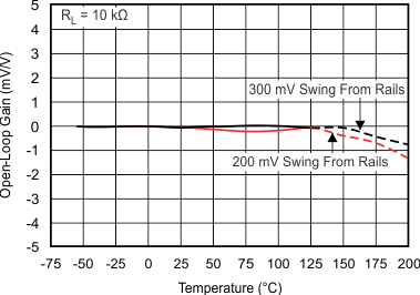
Figure 10.
Open-Loop Gain vs Temperature
Figure 12.
Offset Voltage Drift Production Distribution
Figure 14.
Offset Voltage vs Common-Mode Voltage
Figure 16.
Input Offset Current vs Supply Voltage
Figure 18.
Input Bias Current vs Supply Voltage
Figure 20.
Quiescent Current vs Temperature
Figure 22.
Normalized Quiescent Current vs Time
Figure 24.
Small-Signal Step Response (100 mV)
(100 mV)
Figure 26.
Small-Signal Step Response
(100-mV output step)
Figure 28.
Small-Signal Overshoot vs Capacitive Load
Figure 30.
Large-Signal Step Response
10 V
PP
C
L
= 10 pF
Figure 32.
Large-Signal Positive Settling Time
10 V
PP
C
L
= 10 pF
Figure 34.
Large-Signal Negative Settling Time
Figure 36.
Positive Overload Recovery
Figure 38.
No Phase Reversal
Figure 40.
Turnon Transient