SBOS054C January   1995  – August 2024 OPA132 , OPA2132 , OPA4132

PRODUCTION DATA  

  1.   1
  2. Features
  3. Applications
  4. Description
  5. Pin Configuration and Functions
  6. Specifications
    1. 5.1 Absolute Maximum Ratings
    2. 5.2 ESD Ratings
    3. 5.3 Recommended Operating Conditions
    4. 5.4 Thermal Information - OPA132
    5. 5.5 Thermal Information - OPA2132
    6. 5.6 Thermal Information - OPA4132
    7. 5.7 Electrical Characteristics
    8. 5.8 Typical Characteristics
  7. Detailed Description
    1. 6.1 Overview
    2. 6.2 Functional Block Diagram
    3. 6.3 Feature Description
    4. 6.4 Device Functional Modes
  8. Application and Implementation
    1. 7.1 Application Information
      1. 7.1.1 Operating Voltage
      2. 7.1.2 Offset Voltage Trim
      3. 7.1.3 Input Bias Current
    2. 7.2 Typical Application
      1. 7.2.1 Design Requirements
      2. 7.2.2 Detailed Design Procedure
      3. 7.2.3 Application Curve
    3. 7.3 Power Supply Recommendations
    4. 7.4 Layout
      1. 7.4.1 Layout Guidelines
      2. 7.4.2 Layout Example
  9. Device and Documentation Support
    1. 8.1 Device Support
      1. 8.1.1 Development Support
        1. 8.1.1.1 Analog Filter Designer
        2. 8.1.1.2 TINA-TI™ Simulation Software (Free Download)
        3. 8.1.1.3 TI Reference Designs
    2. 8.2 Documentation Support
      1. 8.2.1 Related Documentation
    3. 8.3 Receiving Notification of Documentation Updates
    4. 8.4 Support Resources
    5. 8.5 Trademarks
    6. 8.6 Electrostatic Discharge Caution
    7. 8.7 Glossary
  10. Revision History
  11. 10Mechanical, Packaging, and Orderable Information

Package Options

Refer to the PDF data sheet for device specific package drawings

Mechanical Data (Package|Pins)
  • D|8
  • P|8
Thermal pad, mechanical data (Package|Pins)
Orderable Information

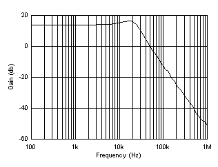
Application Curve

OPA132 OPA2132 OPA4132 OPA132 2nd-Order 30kHz, Low-Pass Filter
                                                  ResponseFigure 7-2 OPA132 2nd-Order 30kHz, Low-Pass Filter Response