SBOS556D June 2011 – August 2020 OPA171-Q1 , OPA2171-Q1 , OPA4171-Q1
PRODUCTION DATA
- 1 Features
- 2 Applications
- 3 Description
- 4 Revision History
- 5 Pin Configuration and Functions
- 6 Specifications
- 7 Detailed Description
- 8 Application and Implementation
- 9 Power Supply Recommendations
- 10Layout
- 11Device and Documentation Support
- 12Mechanical, Packaging, and Orderable Information
Package Options
Mechanical Data (Package|Pins)
Thermal pad, mechanical data (Package|Pins)
Orderable Information
1 Features
- Qualified for automotive applications
- AEC-Q100 test guidance with the following
results:
- Temperature grade 1:
–40°C to +125°C ambient operating temperature - Device HBM ESD
classification level:
- Level 3A for OPA171-Q1
- Level 2 for OPA4171-Q1
- Device CDM ESD
classification level
- Level C4A for OPA171-Q1TLV171-Q1
- Level C6 for OPA2171-Q1
- Level C6 for OPA4171-Q1
- Temperature grade 1:
- Supply range:
- Single-supply: 2.7 V to 36 V
- Dual-supply ±1.35 V to ±18 V
- Low noise: 14 nV/√Hz at 1 kHz
- Low offset drift: ±0.3 µV/°C (typical)
- Input range includes negative supply
- Input range operates to positive supply with reduced performance
- Rail-to-rail output
- Gain bandwidth: 3 MHz
- Low quiescent current: 475 µA per amplifier
- High Common-mode rejection: 120 dB (typical)
- Low input bias current: 10 pA
- Industry-Standard Package:
- 5-Pin Small-Outline Transistor SOT-23 (DBV) Package
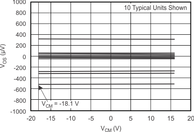
 Offset Voltage vs Common-Mode Voltage:
 VSUPPLY = ±18 V