SBOS861A June   2017  – June 2018 OPA180-Q1 , OPA2180-Q1

PRODUCTION DATA.  

  1. Features
  2. Applications
  3. Description
    1.     Low Noise (Peak-to-Peak Noise = 250 nV)
  4. Revision History
  5. Device Comparison Table
  6. Pin Configuration and Functions
    1.     Pin Functions: OPA180-Q1
    2.     Pin Functions: OPA2180-Q1
  7. Specifications
    1. 7.1 Absolute Maximum Ratings
    2. 7.2 ESD Ratings
    3. 7.3 Recommended Operating Conditions
    4. 7.4 Thermal Information: OPA180-Q1
    5. 7.5 Thermal Information: OPA2180-Q1
    6. 7.6 Electrical Characteristics: VS = ±2 V to ±18 V (VS = 4 V to 36 V)
    7. 7.7 Typical Characteristics: Table of Graphs
    8. 7.8 Typical Characteristics
  8. Detailed Description
    1. 8.1 Overview
    2. 8.2 Functional Block Diagram
    3. 8.3 Feature Description
      1. 8.3.1 Operating Characteristics
      2. 8.3.2 EMI Rejection
      3. 8.3.3 Phase-Reversal Protection
      4. 8.3.4 Capacitive Load and Stability
      5. 8.3.5 Electrical Overstress
    4. 8.4 Device Functional Modes
  9. Application and Implementation
    1. 9.1 Application Information
    2. 9.2 Typical Applications
      1. 9.2.1 Bipolar ±10-V Analog Output from a Unipolar Voltage Output DAC
        1. 9.2.1.1 Design Requirements
        2. 9.2.1.2 Detailed Design Procedure
          1. 9.2.1.2.1 Component Selection
        3. 9.2.1.3 Application Curves
      2. 9.2.2 Discrete INA + Attenuation
      3. 9.2.3 RTD Amplifier
  10. 10Power Supply Recommendations
  11. 11Layout
    1. 11.1 Layout Guidelines
    2. 11.2 Layout Example
  12. 12Device and Documentation Support
    1. 12.1 Related Links
    2. 12.2 Trademarks
    3. 12.3 Electrostatic Discharge Caution
    4. 12.4 Glossary
  13. 13Mechanical, Packaging, and Orderable Information

Package Options

Mechanical Data (Package|Pins)
Thermal pad, mechanical data (Package|Pins)
Orderable Information

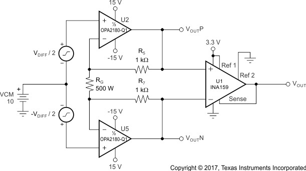
Discrete INA + Attenuation

The OPAx180-Q1 family can be used as a high-voltage, high-impedance front-end for a precision, discrete instrumentation amplifier with attenuation. The INA159 inFigure 33 provides the attenuation that allows this circuit to simply interface with 3.3-V or 5-V analog-to-digital converters (ADCs).
OPA180-Q1 OPA2180-Q1 ai_discrete_sbos861.gifFigure 33. Discrete INA + Attenuation for ADC With a 3.3-V Supply