SBOS525C August 2011 – June 2016 OPA2188
PRODUCTION DATA.
- 1 Features
- 2 Applications
- 3 Description
- 4 Revision History
- 5 Zero-Drift Amplifier Portfolio
- 6 Pin Configuration and Functions
-
7 Specifications
- 7.1 Absolute Maximum Ratings
- 7.2 ESD Ratings
- 7.3 Recommended Operating Conditions
- 7.4 Thermal Information
- 7.5 Electrical Characteristics: High-Voltage Operation, VS = ±4 V to ±18 V (VS = 8 V to 36 V)
- 7.6 Electrical Characteristics: Low-Voltage Operation, VS = ±2 V to < ±4 V (VS = +4 V to < +8 V)
- 7.7 Typical Characteristics: Table of Graphs
- 7.8 Typical Characteristics
- 8 Detailed Description
- 9 Application and Implementation
- 10Power Supply Recommendations
- 11Layout
- 12Device and Documentation Support
- 13Mechanical, Packaging, and Orderable Information
Package Options
Mechanical Data (Package|Pins)
Thermal pad, mechanical data (Package|Pins)
Orderable Information
7 Specifications
7.1 Absolute Maximum Ratings
over operating free-air temperature range (unless otherwise noted)(1)| MIN | MAX | UNIT | ||
|---|---|---|---|---|
| Voltage | Supply voltage | ±20, 40 (single supply) |
V | |
| Signal input terminals, voltage(2) | (V–) – 0.5 | (V+) + 0.5 | V | |
| Current | Signal input terminals, current(2) | –10 | 10 | mA |
| Output short-circuit(3) | Continuous | |||
| Temperature | Operating, TA | –55 | 125 | °C |
| Junction, TJ | 150 | °C | ||
| Storage, Tstg | –65 | 150 | °C | |
(1) Stresses beyond those listed under Absolute Maximum Ratings may cause permanent damage to the device. These are stress ratings only, which do not imply functional operation of the device at these or any other conditions beyond those indicated under Recommended Operating Conditions. Exposure to absolute-maximum-rated conditions for extended periods may affect device reliability.
(2) Input terminals are diode-clamped to the power-supply rails. Input signals that can swing more than 0.5 V beyond the supply rails should be current-limited to 10 mA or less.
(3) Short-circuit to ground, one amplifier per package.
7.2 ESD Ratings
| VALUE | UNIT | |||
|---|---|---|---|---|
| V(ESD) | Electrostatic discharge | Human-body model (HBM), per ANSI/ESDA/JEDEC JS-001(1) | ±1500 | V |
| Charged-device model (CDM), per JEDEC specification JESD22-C101(2) | ±1000 | |||
(1) JEDEC document JEP155 states that 500-V HBM allows safe manufacturing with a standard ESD control process.
(2) JEDEC document JEP157 states that 250-V CDM allows safe manufacturing with a standard ESD control process.
7.3 Recommended Operating Conditions
over operating free-air temperature range (unless otherwise noted)| MIN | NOM | MAX | UNIT | ||
|---|---|---|---|---|---|
| VS | Supply voltage | 4 (±2) | 36 (±18) | V | |
| TA | Specified temperature range | -40 | +105 | °C | |
7.4 Thermal Information
| THERMAL METRIC(1) | OPA2188ID | OPA2188IDGK | UNIT | |
|---|---|---|---|---|
| D (SOIC) | DGK (VSSOP) | |||
| 8 PINS | 8 PINS | |||
| RθJA | Junction-to-ambient thermal resistance | 111 | 159.3 | °C/W |
| RθJC(top) | Junction-to-case (top) thermal resistance | 54.9 | 37.4 | °C/W |
| RθJB | Junction-to-board thermal resistance | 51.7 | 48.5 | °C/W |
| ψJT | Junction-to-top characterization parameter | 9.3 | 1.2 | °C/W |
| ψJB | Junction-to-board characterization parameter | 51.1 | 77.1 | °C/W |
| RθJC(bot) | Junction-to-case (bottom) thermal resistance | n/a | n/a | °C/W |
(1) For more information about traditional and new thermal metrics, see Semiconductor and IC Package Thermal Metrics.
7.5 Electrical Characteristics: High-Voltage Operation, VS = ±4 V to ±18 V (VS = 8 V to 36 V)
at TA = 25°C, RL = 10 kΩ connected to VS/2, and VCOM = VOUT = VS/2, unless otherwise noted.| PARAMETER | TEST CONDITIONS | MIN | TYP | MAX | UNIT | ||
|---|---|---|---|---|---|---|---|
| OFFSET VOLTAGE | |||||||
| VOS | Input offset voltage | 6 | 25 | μV | |||
| TA = –40°C to +105°C | 0.03 | 0.085 | μV/°C | ||||
| PSRR | Power-supply rejection ratio | VS = 4 V to 36 V, VCM = VS / 2 | 0.075 | 0.3 | μV/V | ||
| VS = 4 V to 36 V, VCM = VS / 2, TA = –40°C to +105°C |
0.3 | μV/V | |||||
| Long-term stability | 4(1) | μV | |||||
| Channel separation, DC | 1 | μV/V | |||||
| INPUT BIAS CURRENT | |||||||
| IB | Input bias current | VCM = VS / 2 | ±160 | ±850 | pA | ||
| TA = –40°C to +105°C | ±18 | nA | |||||
| IOS | Input offset current | ±320 | ±1700 | pA | |||
| TA = –40°C to +105°C | ±6 | nA | |||||
| NOISE | |||||||
| en | Input voltage noise | f = 0.1 Hz to 10 Hz | 0.25 | μVPP | |||
| en | Input voltage noise density | f = 1 kHz | 8.8 | nV/√Hz | |||
| in | Input current noise density | f = 1 kHz | 7 | fA/√Hz | |||
| INPUT VOLTAGE RANGE | |||||||
| VCM | Common-mode voltage | V– | (V+) – 1.5 | V | |||
| CMRR | Common-mode rejection ratio | (V–) < VCM < (V+) – 1.5 V | 120 | 134 | dB | ||
| (V–) + 0.5 V < VCM < (V+) – 1.5 V, VS = ±18 V |
130 | 146 | dB | ||||
| (V–) + 0.5 V < VCM < (V+) – 1.5 V, VS = ±18 V, TA = –40°C to +105°C |
120 | 126 | dB | ||||
| INPUT IMPEDANCE | |||||||
| Differential | 100 || 6 | MΩ || pF | |||||
| Common-mode | 6 || 9.5 | 1012 Ω || pF | |||||
| OPEN-LOOP GAIN | |||||||
| AOL | Open-loop voltage gain | (V–) + 500 mV < VO < (V+) – 500 mV, RL = 10 kΩ |
130 | 136 | dB | ||
| (V–) + 500 mV < VO < (V+) – 500 mV, RL = 10 kΩ, TA = –40°C to +105°C |
120 | 126 | dB | ||||
| FREQUENCY RESPONSE | |||||||
| GBW | Gain-bandwidth product | 2 | MHz | ||||
| SR | Slew rate | G = +1 | 0.8 | V/μs | |||
| Settling time, 0.1% | VS = ±18 V, G = 1, 10-V step | 20 | μs | ||||
| Settling time, 0.01% | VS = ±18 V, G = 1, 10-V step | 27 | μs | ||||
| Overload recovery time | VIN × G = VS | 1 | μs | ||||
| THD+N | Total harmonic distortion + noise | 1 kHz, G = 1, VOUT = 1 VRMS | 0.0001 | % | |||
| OUTPUT | |||||||
| Voltage output swing from rail | No load | 6 | 15 | mV | |||
| RL = 10 kΩ | 220 | 250 | mV | ||||
| RL = 10 kΩ, TA = –40°C to +105°C | 310 | 350 | mV | ||||
| ISC | Short-circuit current | ±18 | mA | ||||
| RO | Open-loop output resistance | f = 1 MHz, IO = 0 | 120 | Ω | |||
| CLOAD | Capacitive load drive | 1 | nF | ||||
| POWER SUPPLY | |||||||
| VS | Operating voltage | 4 to 36 (±2 to ±18) | V | ||||
| IQ | Quiescent current (per amplifier) | VS = ±4 V to VS = ±18 V | 415 | 510 | μA | ||
| IO = 0 mA, TA = –40°C to +105°C | 600 | μA | |||||
(1) 1000-hour life test at +125°C demonstrated randomly distributed variation in the range of measurement limits—approximately 4 μV.
7.6 Electrical Characteristics: Low-Voltage Operation, VS = ±2 V to < ±4 V (VS = +4 V to < +8 V)
at TA = 25°C, RL = 10 kΩ connected to VS/2, and VCOM = VOUT = VS/2, unless otherwise noted.| PARAMETER | TEST CONDITIONS | MIN | TYP | MAX | UNIT | ||
|---|---|---|---|---|---|---|---|
| OFFSET VOLTAGE | |||||||
| VOS | Input offset voltage | 6 | 25 | μV | |||
| TA = –40°C to +105°C | 0.03 | 0.085 | μV/°C | ||||
| PSRR | Power-supply rejection ratio | VS = 4 V to 36 V, VCM = VS / 2 | 0.075 | 0.3 | μV/V | ||
| VS = 4 V to 36 V, VCM = VS / 2, TA = –40°C to +105°C |
0.3 | μV/V | |||||
| Long-term stability | 4(1) | μV | |||||
| Channel separation, dc | 1 | μV/V | |||||
| INPUT BIAS CURRENT | |||||||
| IB | Input bias current | VCM = VS / 2 | ±160 | ±850 | pA | ||
| TA = –40°C to +105°C | ±18 | nA | |||||
| IOS | Input offset current | ±320 | ±1700 | pA | |||
| TA = –40°C to +105°C | ±6 | nA | |||||
| NOISE | |||||||
| en | Input voltage noise | f = 0.1 Hz to 10 Hz | 0.25 | μVPP | |||
| Input voltage noise density | f = 1 kHz | 8.8 | nV/√Hz | ||||
| in | Input current noise density | f = 1 kHz | 7 | fA/√Hz | |||
| INPUT VOLTAGE RANGE | |||||||
| VCM | Common-mode voltage range | TA = –40°C to +105°C | V– | (V+) – 1.5 | V | ||
| CMRR | Common-mode rejection ratio | (V–) < VCM < (V+) – 1.5 V | 106 | 114 | dB | ||
| (V–) + 0.5 V < VCM < (V+) – 1.5 V, VS = ±2 V |
114 | 120 | dB | ||||
| (V–) + 0.5 V < VCM < (V+) – 1.5 V, VS = ±2 V, TA = –40°C to +105°C |
110 | 120 | dB | ||||
| INPUT IMPEDANCE | |||||||
| Differential | 100 || 6 | MΩ || pF | |||||
| Common-mode | 6 || 95 | 1012 Ω || pF | |||||
| OPEN-LOOP GAIN | |||||||
| AOL | Open-loop voltage gain | (V–) + 500 mV < VO < (V+) – 500 mV, RL = 5 kΩ, VS = 5 V |
110 | 120 | dB | ||
| (V–) + 500 mV < VO < (V+) – 500 mV, RL = 10 kΩ |
120 | 130 | dB | ||||
| (V–) + 500 mV < VO < (V+) – 500 mV, RL = 10 kΩ, TA = –40°C to +105°C |
114 | 120 | dB | ||||
| FREQUENCY RESPONSE | |||||||
| GBW | Gain-bandwidth product | 2 | MHz | ||||
| SR | Slew rate | G = +1 | 0.8 | V/μs | |||
| Overload recovery time | VIN × G = VS | 1 | μs | ||||
| THD+N | Total harmonic distortion + noise | 1 kHz, G = 1, VOUT = 1 VRMS | 0.0001 | % | |||
| OUTPUT | |||||||
| Voltage output swing from rail | No load | 6 | 15 | mV | |||
| RL = 10 kΩ | 220 | 250 | mV | ||||
| RL = 10 kΩ, TA = –40°C to +105°C | 310 | 350 | mV | ||||
| ISC | Short-circuit current | ±18 | mA | ||||
| RO | Open-loop output resistance | f = 1 MHz, IO = 0 | 120 | Ω | |||
| CLOAD | Capacitive load drive | 1 | nF | ||||
| POWER SUPPLY | |||||||
| VS | Operating voltage range | 4 to 36 (±2 to ±18) | V | ||||
| IQ | Quiescent current (per amplifier) | VS = ±2 V to VS = ±4 V | 385 | 485 | μA | ||
| IO = 0 mA, TA = –40°C to +105°C | 590 | μA | |||||
| TEMPERATURE RANGE | |||||||
| Specified temperature range | –40 | 105 | °C | ||||
| TA | Operating temperature range | –40 | 125 | °C | |||
| Tstg | Storage temperature | –65 | 150 | °C | |||
(1) 1000-hour life test at +125°C demonstrated randomly distributed variation in the range of measurement limits—approximately 4 μV.
7.7 Typical Characteristics: Table of Graphs
Table 1. Characteristic Performance Measurements
| DESCRIPTION | FIGURE NO. |
|---|---|
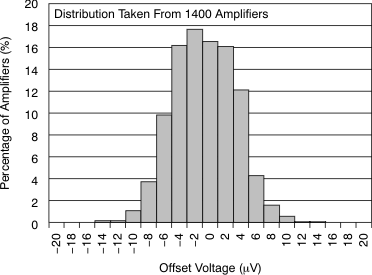
| Offset Voltage Production Distribution | Figure 1 |
| Offset Voltage Drift Distribution | Figure 2 |
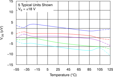
| Offset Voltage vs Temperature | Figure 3 |
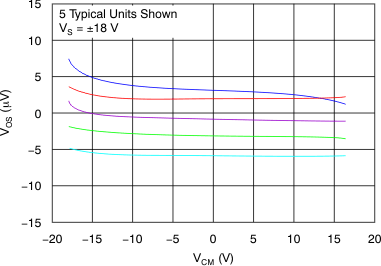
| Offset Voltage vs Common-Mode Voltage | Figure 4, Figure 5 |
| Offset Voltage vs Power Supply | Figure 6 |
| IB and IOS vs Common-Mode Voltage | Figure 7 |
| Input Bias Current vs Temperature | Figure 8 |
| Output Voltage Swing vs Output Current (Maximum Supply) | Figure 9 |
| CMRR and PSRR vs Frequency (Referred-to-Input) | Figure 10 |
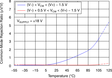
| CMRR vs Temperature | Figure 11, Figure 12 |
| PSRR vs Temperature | Figure 13 |
| 0.1-Hz to 10-Hz Noise | Figure 14 |
| Input Voltage Noise Spectral Density vs Frequency | Figure 15 |
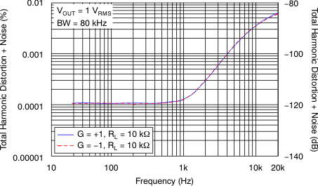
| THD+N Ratio vs Frequency | Figure 16 |
| THD+N vs Output Amplitude | Figure 17 |
| Quiescent Current vs Supply Voltage | Figure 18 |
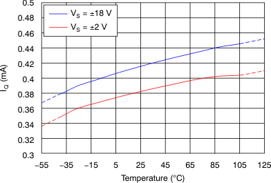
| Quiescent Current vs Temperature | Figure 19 |
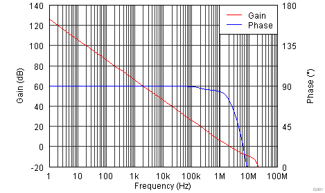
| Open-Loop Gain and Phase vs Frequency | Figure 20 |
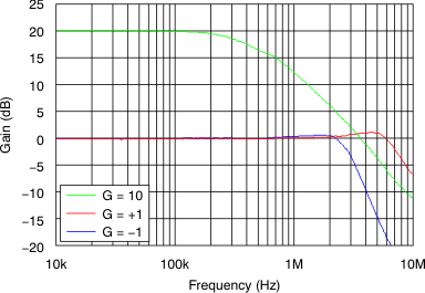
| Closed-Loop Gain vs Frequency | Figure 21 |
| Open-Loop Gain vs Temperature | Figure 22 |
| Open-Loop Output Impedance vs Frequency | Figure 23 |
| Small-Signal Overshoot vs Capacitive Load (100-mV Output Step) | Figure 24, Figure 25 |
| No Phase Reversal | Figure 26 |
| Positive Overload Recovery | Figure 27 |
| Negative Overload Recovery | Figure 28 |
| Small-Signal Step Response (100 mV) | Figure 29, Figure 30 |
| Large-Signal Step Response | Figure 31, Figure 32 |
| Large-Signal Settling Time (10-V Positive Step) | Figure 33 |
| Large-Signal Settling Time (10-V Negative Step) | Figure 34 |
| Short-Circuit Current vs Temperature | Figure 35 |
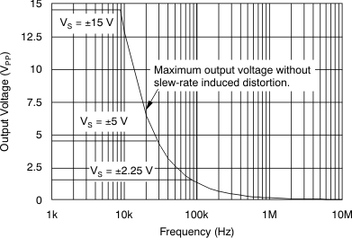
| Maximum Output Voltage vs Frequency | Figure 36 |
| Channel Separation vs Frequency | Figure 37 |
| EMIRR IN+ vs Frequency | Figure 38 |
7.8 Typical Characteristics
VS = ±18 V, VCM = VS/2, RLOAD = 10 kΩ connected to VS/2, and CL = 100 pF, unless otherwise noted.
 Figure 1. Offset Voltage Production Distribution
 Figure 3. Offset Voltage vs Temperature
 Figure 5. Offset Voltage vs Common-Mode Voltage
 Figure 7. IB and IOS vs Common-Mode Voltage
 Figure 9. Output Voltage Swing vs Output Current (Maximum Supply)
 Figure 11. CMRR vs Temperature
 Figure 13. PSRR vs Temperature
 Figure 15. Input Voltage Noise Spectral Density vs Frequency
 Figure 17. THD+N vs Output Amplitude
 Figure 19. Quiescent Current vs Temperature
 Figure 21. Closed-Loop Gain vs Frequency
 Figure 23. Open-Loop Output Impedance vs Frequency
 Figure 25. Small-Signal Overshoot vs Capacitive Load (100-mV Output Step)
 Figure 27. Positive Overload Recovery
 Figure 29. Small-Signal Step Response (100 mV)
 Figure 31. Large-Signal Step Response
 Figure 33. Large-Signal Settling Time (10-V Positive Step)
 Figure 35. Short-Circuit Current vs Temperature
 Figure 37. Channel Separation vs Frequency
 Figure 2. Offset Voltage Drift Distribution
 Figure 4. Offset Voltage vs Common-Mode Voltage
 Figure 6. Offset Voltage vs Power Supply
 Figure 8. Input Bias Current vs Temperature
 Figure 10. CMRR and PSRR vs Frequency (Referred-to-Input)
 Figure 12. CMRR vs Temperature
 Figure 14. 0.1-Hz to 10-Hz Noise
 Figure 16. THD+N Ratio vs Frequency
 Figure 18. Quiescent Current vs Supply Voltage
 Figure 20. Open-Loop Gain and Phase vs Frequency
 Figure 22. Open-Loop Gain vs Temperature
 Figure 24. Small-Signal Overshoot vs Capacitive Load (100-mV Output Step)
 Figure 26. No Phase Reversal
 Figure 28. Negative Overload Recovery
 Figure 30. Small-Signal Step Response (100 mV)
 Figure 32. Large-Signal Step Response
 Figure 34. Large-Signal Settling Time (10-V Negative Step)
 Figure 36. Maximum Output Voltage vs Frequency
 Figure 38. EMIRR IN+ vs Frequency
