SBOS426D November 2008 – October 2016 OPA209 , OPA2209 , OPA4209
PRODUCTION DATA.
- 1 Features
- 2 Applications
- 3 Description
- 4 Revision History
- 5 Pin Configuration and Functions
- 6 Specifications
- 7 Detailed Description
- 8 Application and Implementation
- 9 Power Supply Recommendations
- 10Layout
- 11Device and Documentation Support
- 12Mechanical, Packaging, and Orderable Information
Package Options
Mechanical Data (Package|Pins)
Thermal pad, mechanical data (Package|Pins)
Orderable Information
1 Features
- Low Voltage Noise: 2.2 nV/√Hz at 1 kHz
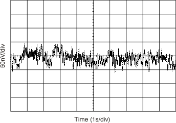
- 0.1-Hz to 10-Hz Noise: 130 nVPP
- Low Quiescent Current: 2.5 mA/Ch (Maximum)
- Low Offset Voltage: 150 µV (Maximum)
- Gain Bandwidth Product: 18 MHz
- Slew Rate: 6.4 V/µs
- Wide Supply Range:
±2.25 V to ±18 V, 4.5 V to 36 V - Rail-to-Rail Output
- Short-Circuit Current: ±65 mA
- Available in 5-Pin SOT-23, 8-Pin MSOP,
8-Pin SOIC, and 14-Pin TSSOP Packages
2 Applications
- PLL Loop Filters
- Low-Noise, Low-Power Signal Processing
- Low-Noise Instrumentation Amplifiers
- High-Performance ADC Drivers
- High-Performance DAC Output Amplifiers
- Active Filters
- Ultrasound Amplifiers
- Professional Audio Preamplifiers
- Low-Noise Frequency Synthesizers
- Infrared Detector Amplifiers
- Hydrophone Amplifiers
3 Description
The OPA209 series of precision operational amplifiers achieve very low voltage noise density
(2.2 nV/√Hz) with a supply current of only 2.5 mA (maximum). This series also offers rail-to-rail output swing, which helps to maximize dynamic range.
In precision data acquisition applications, the OPA209 provides fast settling time to 16-bit accuracy, even for 10-V output swings. This excellent ac performance, combined with only 150 µV (maximum) of offset and low drift over temperature, makes the OPA209 very suitable for fast, high-precision applications.
The OPA209 is specified over a wide dual power-supply range of ±2.25 V to ±18 V, or single-supply operation from 4.5 V to 36 V.
The OPA209 is available in the 5-pin SOT-23, 8-pin VSSOP, and the standard 8-pin SOIC packages. The dual OPA2209 comes in both 8-pin VSSOP and 8-pin SOIC packages. The quad OPA4209 is available in the 14-pin TSSOP package.
The OPA209 series is specified from –40°C to 125°C.
Device Information(1)
| PART NUMBER | PACKAGE | BODY SIZE (NOM) |
|---|---|---|
| OPA209 | SOT-23 (5) | 2.90 mm × 1.60 mm |
| VSSOP (8) | 3.00 mm × 3.00 mm | |
| SOIC (8) | 4.90 mm × 3.91 mm | |
| OPA2209 | VSSOP (8) | 3.00 mm × 3.00 mm |
| SOIC (8) | 4.90 mm × 3.91 mm | |
| OPA4209 | TSSOP (14) | 5.00 mm × 4.40 mm |
- For all available packages, see the orderable addendum at the end of the data sheet.
0.1-Hz to 10-Hz Noise
