SBOS761 November 2015 OPA2211-EP
PRODUCTION DATA.
- 1 Features
- 2 Applications
- 3 Description
- 4 Revision History
- 5 Pin Configuration and Functions
- 6 Specifications
- 7 Detailed Description
- 8 Application and Implementation
- 9 Power Supply Recommendations
- 10Layout
- 11Device and Documentation Support
- 12Mechanical, Packaging, and Orderable Information
Package Options
Mechanical Data (Package|Pins)
- DRG|8
Thermal pad, mechanical data (Package|Pins)
- DRG|8
Orderable Information
1 Features
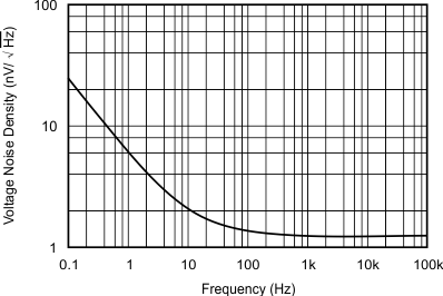
- Low Voltage Noise: 1.1 nV/√Hz at 1 kHz
- Input Voltage Noise: 80 nVPP (0.1 to 10 Hz)
- THD+N: –136 dB (G = 1, ƒ = 1 kHz)
- Offset Voltage: 180 μV (Max)
- Offset Voltage Drift: 0.35 μV/°C (Typ)
- Low Supply Current: 3.6 mA/Ch (Typ)
- Unity-Gain Stable
- Gain Bandwidth Product:
80 MHz (G = 100)
45 MHz (G = 1) - Slew Rate: 27 V/μs
- 16-Bit Settling: 700 ns
- Wide Supply Range:
±2.25 V to ±18 V, +4.5 V to +36 V - Rail-to-Rail Output
- Output Current: 30 mA
-
Supports Defense, Aerospace, and Medical Applications
- Controlled Baseline
- One Assembly and Test Site
- One Fabrication Site
- Available in Military (–55°C to 125°C) Temperature Range (1)
- Extended Product Life Cycle
- Extended Product-Change Notification
- Product Traceability
2 Applications
- PLL Loop Filter
- Low-Noise, Low-Power Signal Processing
- 16-Bit ADC Drivers
- DAC Output Amplifiers
- Active Filters
- Low-Noise Instrumentation Amplifiers
- Ultrasound Amplifiers
- Professional Audio Preamplifiers
- Low-Noise Frequency Synthesizers
- Infrared Detector Amplifiers
- Hydrophone Amplifiers
- Geophone Amplifiers
- Medical
3 Description
The OPA2211-EP series of precision operational amplifiers achieves very-low 1.1-nV/√Hz noise density with a supply current of only 3.6 mA. This series also offers rail-to-rail output swing, which maximizes dynamic range.
The extremely low voltage and low current noise, high speed, and wide output swing of the OPA2211-EP series make these devices an excellent choice as a loop filter amplifier in PLL applications.
In precision data acquisition applications, the OPA2211-EP series of operational amplifiers provides 700-ns settling time to 16-bit accuracy throughout 10-V output swings. This AC performance, combined with only 125 μV of offset and 0.35 μV/°C of drift over temperature, makes the OPA2211-EP ideal for driving high-precision 16-bit analog-to-digital converters (ADCs) or buffering the output of high-resolution digital-to-analog converters (DACs).
The OPA2211-EP is specified over a wide dual-power supply range of ±2.25 V to ±18 V, or for single-supply operation from 4.5 to 36 V.
The OPA2211-EP is available in a small DFN-8 (3-mm × 3-mm) package. These operational amplifiers are specified from TJ = –55°C to 125°C.
Device Information(1)
| PART NUMBER | PACKAGE | BODY SIZE (NOM) |
|---|---|---|
| OPA2211-EP | WSON (8) | 3.00 mm × 3.00 mm |
- For all available packages, see the orderable addendum at the end of the data sheet.
Voltage Noise Density vs Frequency

4 Revision History
| DATE | REVISION | NOTES |
|---|---|---|
| November 2015 | * | Initial release. |