SBOS075A September 2000 – June 2024 OPA2241 , OPA2251 , OPA241 , OPA251 , OPA4241 , OPA4251
PRODUCTION DATA
- 1
- 1Features
- 2Applications
- 3Description
- 4Pin Configuration and Functions
-
5Specifications
- 5.1 Absolute Maximum Ratings
- 5.2 Recommended Operating Conditions
- 5.3 Thermal Information for OPA241 and OPA251
- 5.4 Thermal Information for OPA2241 and OPA2251
- 5.5 Thermal Information for OPA4241 and OPA4251
- 5.6 Electrical Characteristics for VS = 2.7V to 5V
- 5.7 Electrical Characteristics for VS = ±15V
- 5.8 Typical Characteristics
- 6Application and Implementation
- 7Device and Documentation Support
- 8Revision History
- 9Mechanical, Packaging, and Orderable Information
Package Options
Refer to the PDF data sheet for device specific package drawings
Mechanical Data (Package|Pins)
- D|8
- P|8
Thermal pad, mechanical data (Package|Pins)
Orderable Information
4 Pin Configuration and Functions
 Figure 4-1 OPA241 and OPA251: D Package, 8-Pin
SOIC
 and P Package, 8-Pin PDIP (Top View)
Table 4-1 Pin Functions: OPA241 and OPA251
| PIN | TYPE | DESCRIPTION | |
|---|---|---|---|
| NAME | NO. | ||
| +IN | 3 | Input | Noninverting input |
| –IN | 2 | Input | Inverting input |
| NC | 8 | — | No internal connection (can be left floating) |
| OUT | 6 | Output | Output |
| TRIM | 1, 5 | — | External offset voltage adjustment. See Section 6.1.2. |
| V+ | 7 | Power | Positive (highest) power supply |
| V– | 4 | Power | Negative (lowest) power supply |
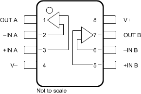
 Figure 4-2 OPA2241 and OPA2251: D Package, 8-Pin
SOIC,
 and P Package, 8-Pin PDIP (Top View)
Table 4-2 Pin Functions: OPA2241 and OPA2251
| PIN | TYPE | DESCRIPTION | |
|---|---|---|---|
| NAME | NO. | ||
| +IN A | 3 | Input | Noninverting input, channel A |
| +IN B | 5 | Input | Noninverting input, channel B |
| –IN A | 2 | Input | Inverting input, channel A |
| –IN B | 6 | Input | Inverting input, channel B |
| OUT A | 1 | Output | Output, channel A |
| OUT B | 7 | Output | Output, channel B |
| V+ | 8 | Power | Positive (highest) power supply |
| V– | 4 | Power | Negative (lowest) power supply |
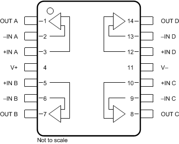
 Figure 4-3 OPA4241 and OPA4251: D Package, 14-Pin
SOIC (Top View)
Figure 4-3 OPA4241 and OPA4251: D Package, 14-Pin
SOIC (Top View)Pin Functions: OPA4241 and
OPA4251
| PIN | TYPE | DESCRIPTION | |
|---|---|---|---|
| NAME | NO. | ||
| +IN A | 3 | Input | Noninverting input, channel A |
| +IN B | 5 | Input | Noninverting input, channel B |
| +IN C | 10 | Input | Noninverting input, channel C |
| +IN D | 12 | Input | Noninverting input, channel D |
| –IN A | 2 | Input | Inverting input, channel A |
| –IN B | 6 | Input | Inverting input, channel B |
| –IN C | 9 | Input | Inverting input, channel C |
| –IN D | 13 | Input | Inverting input, channel D |
| OUT A | 1 | Output | Output, channel A |
| OUT B | 7 | Output | Output, channel B |
| OUT C | 8 | Output | Output, channel C |
| OUT D | 14 | Output | Output, channel D |
| V+ | 4 | Power | Positive (highest) power supply |
| V– | 11 | Power | Negative (lowest) power supply |