SBOS703F April 2014 – October 2016 OPA2316 , OPA316 , OPA4316
PRODUCTION DATA.
- 1 Features
- 2 Applications
- 3 Description
- 4 Revision History
- 5 Pin Configuration and Functions
- 6 Specifications
- 7 Detailed Description
- 8 Application and Implementation
- 9 Power Supply Recommendations
- 10Layout
- 11Device and Documentation Support
- 12Mechanical, Packaging, and Orderable Information
- 11Mechanical, Packaging, and Orderable Information
Package Options
Mechanical Data (Package|Pins)
Thermal pad, mechanical data (Package|Pins)
Orderable Information
6 Specifications
6.1 Absolute Maximum Ratings
over operating free-air temperature (unless otherwise noted)(1)| MIN | MAX | UNIT | |||
|---|---|---|---|---|---|
| Supply voltage | 7 | V | |||
| Signal input pins | Voltage(2) | Common-mode | (V–) – 0.5 | (V+) + 0.5 | V |
| Differential | (V+) – (V–) + 0.2 | V | |||
| Current(2) | –10 | 10 | mA | ||
| Output short-circuit(3) | Continuous | ||||
| TA | Operating temperature | –55 | 150 | °C | |
| TJ | Junction temperature | 150 | °C | ||
| Tstg | Storage temperature | –65 | 150 | °C | |
(1) Stresses beyond those listed under Absolute Maximum Ratings may cause permanent damage to the device. These are stress ratings only, which do not imply functional operation of the device at these or any other conditions beyond those indicated under Recommended Operating Conditions. Exposure to absolute-maximum-rated conditions for extended periods may affect device reliability.
(2) Input pins are diode-clamped to the power-supply rails. Current limit input signals that can swing more than 0.5 V beyond the supply rails to 10 mA or less.
(3) Short-circuit to ground, one amplifier per package.
6.2 ESD Ratings
over operating free-air temperature range (unless otherwise noted).| VALUE | UNIT | |||
|---|---|---|---|---|
| V(ESD) | Electrostatic discharge | Human body model (HBM), per ANSI/ESDA/JEDEC JS-001(1) | ±4000 | V |
| Charged device model (CDM), per JEDEC specification JESD22-C101(2) | ±1500 | |||
(1) JEDEC document JEP155 states that 500-V HBM allows safe manufacturing with a standard ESD control process.
(2) JEDEC document JEP157 states that 250-V CDM allows safe manufacturing with a standard ESD control process.
6.3 Recommended Operating Conditions
over operating free-air temperature range (unless otherwise noted).| MIN | MAX | UNIT | |||
|---|---|---|---|---|---|
| VS | Supply voltage | 1.8 | 5.5 | V | |
| Specified temperature | –40 | 125 | °C | ||
6.4 Thermal Information: OPA316
| THERMAL METRIC(1) | OPA316 | UNIT | ||
|---|---|---|---|---|
| DBV (SOT23) | DCK (SC70) | |||
| 5 PINS | 5 PINS | |||
| RθJA | Junction-to-ambient thermal resistance(2) | 221.7 | 263.3 | °C/W |
| RθJC(top) | Junction-to-case(top) thermal resistance(3) | 144.7 | 75.5 | °C/W |
| RθJB | Junction-to-board thermal resistance(4) | 49.7 | 51 | °C/W |
| ψJT | Junction-to-top characterization parameter(5) | 26.1 | 1 | °C/W |
| ψJB | Junction-to-board characterization parameter(6) | 49 | 50.3 | °C/W |
| RθJC(bot) | Junction-to-case(bottom) thermal resistance(7) | N/A | N/A | °C/W |
(1) For more information about traditional and new thermal metrics, see Semiconductor and IC Package Thermal Metrics (SPRA953).
(2) The junction-to-ambient thermal resistance under natural convection is obtained in a simulation on a JEDEC-standard, high-K board, as specified in JESD51-7, in an environment described in JESD51-2a.
(3) The junction-to-case (top) thermal resistance is obtained by simulating a cold plate test on the package top. No specific JEDEC-standard test exists, but a close description can be found in the ANSI SEMI standard G30-88.
(4) The junction-to-board thermal resistance is obtained by simulating in an environment with a ring cold plate fixture to control the PCB temperature, as described in JESD51-8.
(5) The junction-to-top characterization parameter, ψJT, estimates the junction temperature of a device in a real system and is extracted from the simulation data for obtaining RθJA, using a procedure described in JESD51-2a (sections 6 and 7).
(6) The junction-to-board characterization parameter, ψJB, estimates the junction temperature of a device in a real system and is extracted from the simulation data for obtaining RθJA, using a procedure described in JESD51-2a (sections 6 and 7).
(7) The junction-to-case (bottom) thermal resistance is obtained by simulating a cold plate test on the exposed (power) pad. No specific JEDEC standard test exists, but a close description can be found in the ANSI SEMI standard G30-88.
6.5 Thermal Information: OPA2316
| THERMAL METRIC(1) | OPA2316 | UNIT | |||
|---|---|---|---|---|---|
| D (SO) | DGK (MSOP) | DRG (DFN) | |||
| 8 PINS | 8 PINS | 8 PINS | |||
| RθJA | Junction-to-ambient thermal resistance(2) | 127.2 | 186.6 | 56.3 | °C/W |
| RθJC(top) | Junction-to-case(top) thermal resistance(3) | 71.6 | 78.8 | 72.2 | °C/W |
| RθJB | Junction-to-board thermal resistance(4) | 68.2 | 107.9 | 31 | °C/W |
| ψJT | Junction-to-top characterization parameter(5) | 22 | 15.5 | 2.3 | °C/W |
| ψJB | Junction-to-board characterization parameter(6) | 67.6 | 106.3 | 21.2 | °C/W |
| RθJC(bot) | Junction-to-case(bottom) thermal resistance(7) | N/A | N/A | 10.9 | °C/W |
(1) For more information about traditional and new thermal metrics, see Semiconductor and IC Package Thermal Metrics (SPRA953).
(2) The junction-to-ambient thermal resistance under natural convection is obtained in a simulation on a JEDEC-standard, high-K board, as specified in JESD51-7, in an environment described in JESD51-2a.
(3) The junction-to-case (top) thermal resistance is obtained by simulating a cold plate test on the package top. No specific JEDEC-standard test exists, but a close description can be found in the ANSI SEMI standard G30-88.
(4) The junction-to-board thermal resistance is obtained by simulating in an environment with a ring cold plate fixture to control the PCB temperature, as described in JESD51-8.
(5) The junction-to-top characterization parameter, ψJT, estimates the junction temperature of a device in a real system and is extracted from the simulation data for obtaining RθJA, using a procedure described in JESD51-2a (sections 6 and 7).
(6) The junction-to-board characterization parameter, ψJB, estimates the junction temperature of a device in a real system and is extracted from the simulation data for obtaining RθJA, using a procedure described in JESD51-2a (sections 6 and 7).
(7) The junction-to-case (bottom) thermal resistance is obtained by simulating a cold plate test on the exposed (power) pad. No specific JEDEC standard test exists, but a close description can be found in the ANSI SEMI standard G30-88.
6.6 Thermal Information: OPA2316S
| THERMAL METRIC(1) | OPA2316S | UNIT | ||
|---|---|---|---|---|
| DGS (MSOP) | QFN (RUG) | |||
| 10 PINS | 10 PINS | |||
| RθJA | Junction-to-ambient thermal resistance(2) | 189.6 | 158 | °C/W |
| RθJC(top) | Junction-to-case(top) thermal resistance(3) | 73.9 | 52 | °C/W |
| RθJB | Junction-to-board thermal resistance(4) | 110.7 | 88 | °C/W |
| ψJT | Junction-to-top characterization parameter(5) | 13.4 | 1 | °C/W |
| ψJB | Junction-to-board characterization parameter(6) | 109.1 | 87 | °C/W |
| RθJC(bot) | Junction-to-case(bottom) thermal resistance(7) | N/A | N/A | °C/W |
(1) For more information about traditional and new thermal metrics, see Semiconductor and IC Package Thermal Metrics (SPRA953).
(2) The junction-to-ambient thermal resistance under natural convection is obtained in a simulation on a JEDEC-standard, high-K board, as specified in JESD51-7, in an environment described in JESD51-2a.
(3) The junction-to-case (top) thermal resistance is obtained by simulating a cold plate test on the package top. No specific JEDEC-standard test exists, but a close description can be found in the ANSI SEMI standard G30-88.
(4) The junction-to-board thermal resistance is obtained by simulating in an environment with a ring cold plate fixture to control the PCB temperature, as described in JESD51-8.
(5) The junction-to-top characterization parameter, ψJT, estimates the junction temperature of a device in a real system and is extracted from the simulation data for obtaining RθJA, using a procedure described in JESD51-2a (sections 6 and 7).
(6) The junction-to-board characterization parameter, ψJB, estimates the junction temperature of a device in a real system and is extracted from the simulation data for obtaining RθJA, using a procedure described in JESD51-2a (sections 6 and 7).
(7) The junction-to-case (bottom) thermal resistance is obtained by simulating a cold plate test on the exposed (power) pad. No specific JEDEC standard test exists, but a close description can be found in the ANSI SEMI standard G30-88.
6.7 Thermal Information: OPA4316
| THERMAL METRIC(1) | OPA4316 | UNIT | ||
|---|---|---|---|---|
| PW (TSSOP) | D (SOIC) | |||
| 14 PINS | 14 PINS | |||
| RθJA | Junction-to-ambient thermal resistance(2) | 117.2 | 87.0 | °C/W |
| RθJC(top) | Junction-to-case(top) thermal resistance(3) | 46.2 | 44.4 | °C/W |
| RθJB | Junction-to-board thermal resistance(4) | 58.9 | 41.7 | °C/W |
| ψJT | Junction-to-top characterization parameter(5) | 4.9 | 11.6 | °C/W |
| ψJB | Junction-to-board characterization parameter(6) | 58.3 | 41.4 | °C/W |
| RθJC(bot) | Junction-to-case(bottom) thermal resistance(7) | N/A | N/A | °C/W |
(1) For more information about traditional and new thermal metrics, see Semiconductor and IC Package Thermal Metrics (SPRA953).
(2) The junction-to-ambient thermal resistance under natural convection is obtained in a simulation on a JEDEC-standard, high-K board, as specified in JESD51-7, in an environment described in JESD51-2a.
(3) The junction-to-case (top) thermal resistance is obtained by simulating a cold plate test on the package top. No specific JEDEC-standard test exists, but a close description can be found in the ANSI SEMI standard G30-88.
(4) The junction-to-board thermal resistance is obtained by simulating in an environment with a ring cold plate fixture to control the PCB temperature, as described in JESD51-8.
(5) The junction-to-top characterization parameter, ψJT, estimates the junction temperature of a device in a real system and is extracted from the simulation data for obtaining RθJA, using a procedure described in JESD51-2a (sections 6 and 7).
(6) The junction-to-board characterization parameter, ψJB, estimates the junction temperature of a device in a real system and is extracted from the simulation data for obtaining RθJA, using a procedure described in JESD51-2a (sections 6 and 7).
(7) The junction-to-case (bottom) thermal resistance is obtained by simulating a cold plate test on the exposed (power) pad. No specific JEDEC standard test exists, but a close description can be found in the ANSI SEMI standard G30-88.
6.8 Electrical Characteristics
VS (total supply voltage) = (V+) – (V–) = 1.8 V to 5.5 V.at TA = 25°C, RL = 10 kΩ connected to VS / 2, VCM = VS / 2, and VOUT = VS / 2, unless otherwise noted.
| PARAMETER | TEST CONDITIONS | MIN | TYP | MAX | UNIT | ||
|---|---|---|---|---|---|---|---|
| OFFSET VOLTAGE | |||||||
| VOS | Input offset voltage | VS = 5 V | ±0.5 | ±2.5 | mV | ||
| VS = 5 V, TA = –40°C to 125°C | ±3.5 | mV | |||||
| dVOS/dT | Drift | VS = 5 V, TA = –40°C to 125°C | ±2 | ±10 | μV/°C | ||
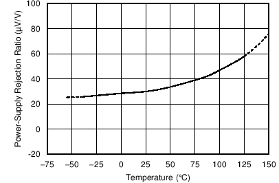
| PSRR | vs power supply | VS = 1.8 V – 5.5 V, VCM = (V–) | ±30 | ±150 | µV/V | ||
| VS = 1.8 V – 5.5 V, VCM = (V–), TA = –40°C to 125°C | ±250 | µV/V | |||||
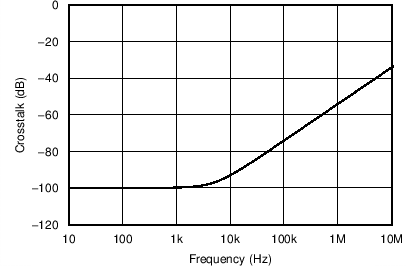
| Channel separation, dc | At dc | 10 | µV/V | ||||
| INPUT VOLTAGE RANGE | |||||||
| VCM | Common-mode voltage | VS = 1.8 V to 2.5 V | (V–) – 0.2 | (V+) | V | ||
| VS = 2.5 V to 5.5 V | (V–) – 0.2 | (V+) + 0.2 | V | ||||
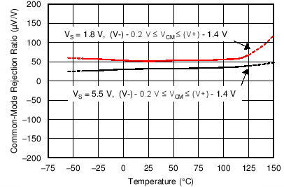
| CMRR | Common-mode rejection ratio | VS = 1.8 V, (V–) – 0.2 V < VCM < (V+) – 1.4 V, TA= –40°C to 125°C |
70 | 86 | dB | ||
| VS = 5.5 V, (V–) – 0.2 V < VCM < (V+) – 1.4 V, TA= –40°C to 125°C |
76 | 90 | dB | ||||
| VS = 1.8 V, VCM = –0.2 V to 1.8 V, TA= –40°C to 125°C |
57 | 72 | dB | ||||
| VS = 5.5 V, VCM = –0.2 V to 5.7 V, TA= –40°C to 125°C |
65 | 80 | dB | ||||
| INPUT BIAS CURRENT | |||||||
| IB | Input bias current | ±5 | ±15 | pA | |||
| TA= –40°C to 125°C | ±15 | nA | |||||
| IOS | Input offset current | ±2 | ±15 | pA | |||
| TA= –40°C to 125°C | ±8 | nA | |||||
| NOISE | |||||||
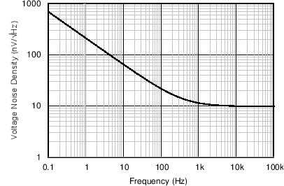
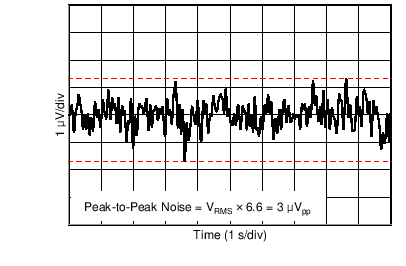
| En | Input voltage noise (peak-to-peak) | VS = 5 V, f = 0.1 Hz to 10 Hz | 3 | μVPP | |||
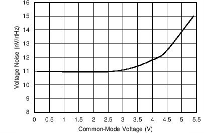
| en | Input voltage noise density | VS = 5 V, f = 1 kHz | 11 | nV/√Hz | |||
| in | Input current noise density | f = 1 kHz | 1.3 | fA/√Hz | |||
| INPUT IMPEDANCE | |||||||
| ZID | Differential | 2 || 2 | 1016Ω || pF | ||||
| ZIC | Common-mode | 2 || 4 | 1011Ω || pF | ||||
| OPEN-LOOP GAIN | |||||||
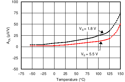
| AOL | Open-loop voltage gain | VS = 1.8 V, (V–) + 0.04 V < VO < (V+) – 0.04 V, RL = 10 kΩ |
94 | 100 | dB | ||
| VS = 5.5 V, (V–) + 0.05 V < VO < (V+) – 0.05 V, RL = 10 kΩ |
104 | 110 | dB | ||||
| VS = 1.8 V, (V–) + 0.1 V < VO < (V+) – 0.1 V, RL = 2 kΩ |
90 | 96 | dB | ||||
| VS = 5.5 V, (V–) + 0.15 V < VO < (V+) – 0.15 V, RL = 2 kΩ |
100 | 106 | dB | ||||
| VS = 5.5 V, (V–) + 0.05 V < VO < (V+) – 0.05 V, RL = 10 kΩ, TA= –40°C to 125°C |
86 | dB | |||||
| VS = 5.5 V, (V–) + 0.15 V < VO < (V+) – 0.15 V, RL = 2 kΩ, TA= –40°C to 125°C |
84 | dB | |||||
| FREQUENCY RESPONSE | |||||||
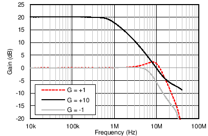
| GBP | Gain bandwidth product | VS = 5 V, G = +1 | 10 | MHz | |||
| φm | Phase margin | VS = 5 V, G = +1 | 60 | Degrees | |||
| SR | Slew rate | VS = 5 V, G = +1 | 6 | V/μs | |||
| tS | Settling time | To 0.1%, VS = 5 V, 2-V step , G = +1, CL = 100 pF | 1 | μs | |||
| To 0.01%, VS = 5 V, 2-V step , G = +1, CL = 100 pF | 1.66 | μs | |||||
| tOR | Overload recovery time | VS = 5 V, VIN × gain = VS | 0.3 | μs | |||
| THD + N | Total harmonic distortion + noise(1) | VS = 5 V, VO = 0.5 VRMS, G = +1, f = 1 kHz | 0.0008% | ||||
| OUTPUT | |||||||
| VO | Voltage output swing from supply rails | VS = 1.8 V, RL = 10 kΩ, TA= –40°C to 125°C | 15 | mV | |||
| VS = 5.5 V, RL = 10 kΩ, TA= –40°C to 125°C | 30 | mV | |||||
| VS = 1.8 V, RL = 2 kΩ, TA= –40°C to 125°C | 60 | mV | |||||
| VS = 5.5 V, RL = 2 kΩ, TA= –40°C to 125°C | 120 | mV | |||||
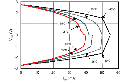
| ISC | Short-circuit current | VS = 5 V | ±50 | mA | |||
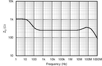
| ZO | Open-loop output impedance | VS = 5 V, f = 10 MHz | 250 | Ω | |||
| POWER SUPPLY | |||||||
| VS | Specified voltage | 1.8 | 5.5 | V | |||
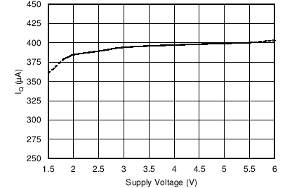
| IQ | Quiescent current per amplifier | VS = 5 V, IO = 0 mA, TA= –40°C to 125°C | 400 | 500 | µA | ||
| Power-on time | VS = 0 V to 5.5 V | 200 | µs | ||||
| SHUTDOWN (VS = 1.8 V to 5.5 V)(2) | |||||||
| IQSD | Quiescent current, per device | All amplifiers disabled, SHDN = VS– | 0.01 | 1 | µA | ||
| One amplifier disabled (OPA2316S) | 345 | µA | |||||
| VIH | High voltage (enabled) | Amplifier enabled | (V+) – 0.5 | V | |||
| VIL | Low voltage (disabled) | Amplifier disabled | (V–) + 0.2 | V | |||
| tON | Amplifier enable time(3) | Full shutdown, G = 1, VOUT = 0.9 × VS / 2(4) | 13 | µs | |||
| Partial shutdown, G = 1, VOUT = 0.9 × VS / 2(4) | 10 | µs | |||||
| tOFF | Amplifier disable time(3) | G = 1, VOUT = 0.1 × VS / 2 | 5 | µs | |||
| SHDN pin input bias current (per pin) | VIH = 5 V | 3.5 | pA | ||||
| VIL = 0 V | 2.5 | pA | |||||
| TEMPERATURE | |||||||
| Specified temperature | –40 | 125 | °C | ||||
| TA | Operating temperature | –55 | 150 | °C | |||
| Tstg | Storage temperature | –65 | 150 | °C | |||
(1) Third-order filter; bandwidth = 80 kHz at –3 dB.
(2) Ensured by design and characterization; not production tested.
(3) Enable time (tON) and disable time (tOFF) are defined as the time interval between the 50% point of the signal applied to the SHDN pin and the point at which the output voltage reaches the 10% (disable) or 90% (enable) level.
(4) Full shutdown refers to the dual OPA2316S having both channels A and B disabled (SHDN_A = SHDN_B = VS–). For partial shutdown, only one SHDN pin is exercised; in partial mode, the internal biasing and oscillator remain operational and the enable time is shorter.
6.9 Typical Characteristics
at TA = 25°C, VS = 5.5 V, RL = 10 kΩ connected to VS / 2, VCM = VS / 2, and VOUT = VS / 2, unless otherwise noted.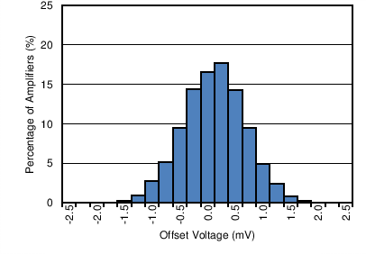
| Distribution taken from 12551 amplifiers | ||
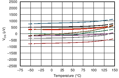
| 9 typical units shown | ||
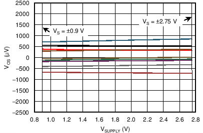
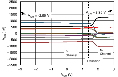
| V+ = 0.9 V to 2.75 V, V– = –0.9 V to –2.75 V, 9 typical units shown |
| RL = 10 kΩ | ||
| V+ = 2.75 V, V– = –2.75 V | ||
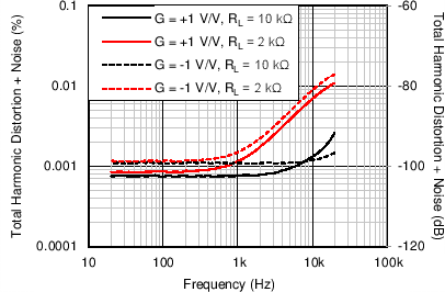
| BW = 80 kHz, VOUT = 0.5 VRMS | ||
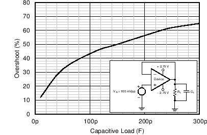
| V+ = 2.75 V, V– = –2.75 V , G = +1 V/V, RL = 1 kΩ | ||
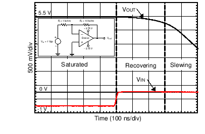
| V+ = 2.75 V, V– = –2.75 V , G = –10 V/V | ||
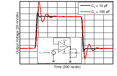
| V+ = 2.75 V, V– = –2.75 V, G = +1 V/V | ||
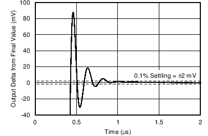
| CL = 100 pF, G = +1 V/V | ||
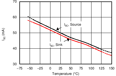
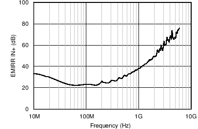
| PRF = –10 dBm | ||
Referred to Noninverting Input (EMIRR IN+) vs Frequency
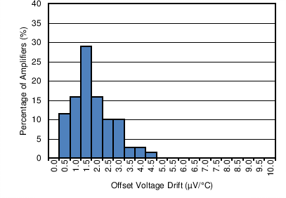
| TA = –40°C to +125°C, Distribution taken from 70 amplifiers | ||
| V+ = 2.75 V, V– = –2.75 V, 9 typical units shown | ||
| VCM < (V+) – 1.4 V | ||
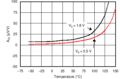
| RL = 2 kΩ | ||
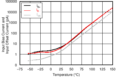
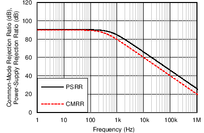
(Referred to Input)
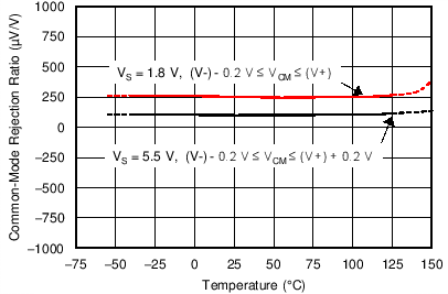
| ƒ = 1 kHz | ||
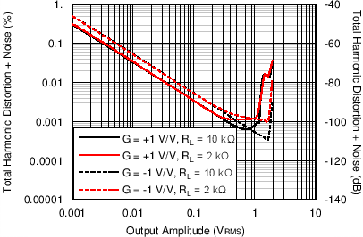
| ƒ = 1 kHz, BW = 80 kHz | ||
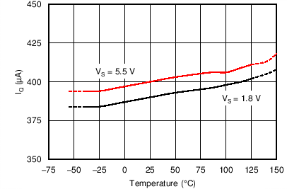
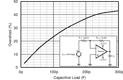
| V+ = 2.75 V, V– = –2.75 V, G = –1 V/V | ||
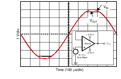
| V+ = 2.75 V, V– = –2.75 V | ||
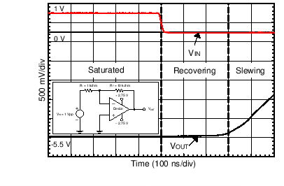
| V+ = 2.75 V, V– = –2.75 V, G = –10 V/V | ||
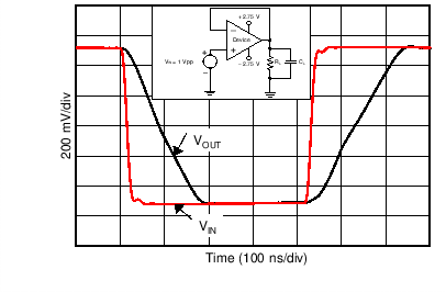
| V+ = 2.75 V, V– = –2.75 V, CL = 100 pF, G = +1 V/V | ||
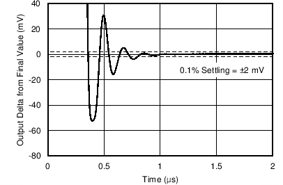
| CL = 100 pF, G = +1 V/V | ||
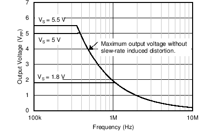
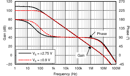
Frequency and Supply Voltage
