SLOS914 July 2016 OPA2317-Q1 , OPA317-Q1
PRODUCTION DATA.
- 1 Features
- 2 Applications
- 3 Description
- 4 Revision History
- 5 Pin Configuration and Functions
- 6 Specifications
- 7 Parameter Measurement Information
- 8 Detailed Description
- 9 Application and Implementation
- 10Power Supply Recommendations
- 11Layout
- 12Device and Documentation Support
- 13Mechanical, Packaging, and Orderable Information
Package Options
Mechanical Data (Package|Pins)
- DGK|8
Thermal pad, mechanical data (Package|Pins)
Orderable Information
8 Detailed Description
8.1 Overview
The OPA317-Q1 is a family of low-power, rail-to-rail input and output operational amplifiers. These devices operate from 1.8 V to 5.5 V, are unity-gain stable, and are suitable for a wide range of general-purpose applications. The class AB output stage is capable of driving ≤ 10-kΩ loads connected to any point between V+ and ground. The input common-mode voltage range includes both rails and allows the OPA317 series to be used in virtually any single-supply application. Rail-to-rail input and output swing significantly increases dynamic range, especially in low-supply applications, and makes them ideal for driving sampling analog-to-digital converters (ADCs).
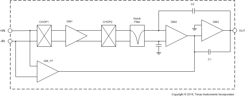
8.2 Functional Block Diagram

8.3 Feature Description
8.3.1 Operating Voltage
The OPA317-Q1 series of operational amplifiers can be used with single or dual supplies from an operating range of VS = 1.8 V (±0.9 V) up to 5.5 V (±2.75 V).
CAUTION
Supply voltages greater than 7 V can permanently damage the device.
See the Absolute Maximum Ratings table. Key parameters that vary over the supply voltage or temperature range are shown in the Typical Characteristics section.
8.3.2 Input Voltage
The OPA317-Q1, OPA2317-Q1, and OPA4317-Q1 input common-mode voltage range extends 0.1 V beyond the supply rails. The OPA317-Q1 device is designed to cover the full range without the troublesome transition region found in some other rail-to-rail amplifiers.
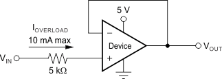
Typically, input bias current is about 200 pA; however, input voltages exceeding the power supplies can cause excessive current to flow into or out of the input pins. Momentary voltages greater than the power supply can be tolerated if the input current is limited to 10 mA. This limitation is easily accomplished with an input resistor, as shown in Figure 19.

8.3.3 Input Differential Voltage
The typical input bias current of the OPA317-Q1 during normal operation is approximately 200 pA. In overdriven conditions, the bias current can increase significantly (see Figure 17).The most common cause of an overdriven condition occurs when the operational amplifier is outside of the linear range of operation. When the output of the operational amplifier is driven to one of the supply rails, the feedback loop requirements cannot be satisfied, and a differential input voltage develops across the input pins. This differential input voltage results in activation of parasitic diodes inside the front-end input chopping switches that combine with 10-kΩ electromagnetic interference (EMI) filter resistors to create the equivalent circuit shown in Figure 20.
NOTE
The input bias current remains within specification within the linear region.
 Figure 20. Equivalent Input Circuit
8.3.4 Internal Offset Correction
The OPA317-Q1, OPA2317-Q1, and OPA4317-Q1 operational amplifiers use an auto-calibration technique with a time-continuous, 125-kHz operational amplifier in the signal path. This amplifier is zero-corrected every 8 μs using a proprietary technique. Upon power up, the amplifier requires approximately 100 μs to achieve specified VOS accuracy. This design has no aliasing or flicker noise.
8.3.5 EMI Susceptibility and Input Filtering
Operational amplifiers vary in susceptibility to EMI. If conducted EMI enters the operational amplifier, the DC offset observed at the amplifier output may shift from its nominal value while the EMI is present. This shift is a result of signal rectification associated with the internal semiconductor junctions. While all operational amplifier pin functions can be affected by EMI, the input pins are likely to be the most susceptible. The OPA317-Q1 operational amplifier family incorporates an internal input low-pass filter that reduces the amplifier response to EMI. Both common-mode and differential mode filtering are provided by the input filter. The filter is designed for a cutoff frequency of approximately 8 MHz (–3 dB), with a roll-off of 20 dB per decade.
8.4 Device Functional Modes
The OPAx317-Q1 family of devices are powered on when the supply is connected. The device can be operated as a single-supply operational amplifier or a dual-supply amplifier, depending on the application.