SBOS957D February 2022 – December 2023 OPA2328 , OPA328
PRODMIX
- 1
- 1 Features
- 2 Applications
- 3 Description
- 4 Pin Configuration and Functions
- 5 Specifications
- 6 Detailed Description
- 7 Application and Implementation
- 8 Device and Documentation Support
- 9 Revision History
- 10Mechanical, Packaging, and Orderable Information
Package Options
Refer to the PDF data sheet for device specific package drawings
Mechanical Data (Package|Pins)
- D|8
- DGK|8
- DRG|8
Thermal pad, mechanical data (Package|Pins)
- DRG|8
Orderable Information
4 Pin Configuration and Functions
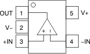 Figure 4-1 OPA328 DBV Package,
 5-Pin SOT-23 (Top View)
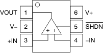 Figure 4-2 OPA328S DBV Package
(Preview)
 6-Pin SOT-23 (Top View)
Pin Functions:
OPA328 and OPA328S
| PIN | TYPE | DESCRIPTION | ||
|---|---|---|---|---|
| NAME | OPA328 | OPA328S | ||
| –IN | 4 | 4 | Input | Negative (inverting) input |
| +IN | 3 | 3 | Input | Positive (noninverting) input |
| OUT, VOUT | 1 | 1 | Output | Output |
| SHDN | — | 5 | Input | Shutdown, active low |
| V– | 2 | 2 | Power | Negative (lowest) power supply |
| V+ | 5 | 6 | Power | Positive (highest) power supply |
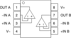 Figure 4-3 OPA2328 D Package, 8-pin
SOIC and DGK Package, 8-Pin VSSOP (Top View)
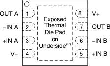 Figure 4-4 OPA2328 DRG Package,
 8-Pin WSON (Top View)
Pin Functions:
OPA2328
| PIN | TYPE | DESCRIPTION | |
|---|---|---|---|
| NAME | NO. | ||
| –IN A | 2 | Input | Inverting input, channel A |
| +IN A | 3 | Input | Noninverting input, channel A |
| –IN B | 6 | Input | Inverting input, channel B |
| +IN B | 5 | Input | Noninverting input, channel B |
| OUT A | 1 | Output | Output, channel A |
| OUT B | 7 | Output | Output, channel B |
| V– | 4 | Power | Negative (lowest) power supply |
| V+ | 8 | Power | Positive (highest) power supply |
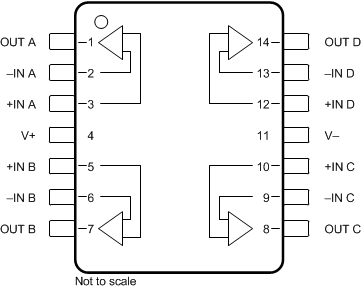 Figure 4-5 OPA4328 PW Package
(Preview), 14-Pin TSSOP (Top View)
Figure 4-6 OPA4328 RUM Package
(Preview), 16-Pin WQFN (Top View)
Table 4-1 Pin Functions: OPA4328
| PIN | TYPE | DESCRIPTION | ||
|---|---|---|---|---|
| NAME | NO. | |||
| PW (TSSOP) | RUM (WQFN) | |||
| EN AB | — | 6 | Input | Enable pin for A and B amplifiers. High = amplifiers A and B are enabled. |
| EN CD | — | 7 | Input | Enable pin for C and D amplifiers. High = amplifiers C and D are enabled. |
| –IN A | 2 | 16 | Input | Inverting input, channel A |
| +IN A | 3 | 1 | Input | Noninverting input, channel A |
| –IN B | 6 | 4 | Input | Inverting input, channel B |
| +IN B | 5 | 3 | Input | Noninverting input, channel B |
| –IN C | 9 | 9 | Input | Inverting input, channel C |
| +IN C | 10 | 10 | Input | Noninverting input, channel C |
| –IN D | 13 | 13 | Input | Inverting input, channel D |
| +IN D | 12 | 12 | Input | Noninverting input, channel D |
| OUT A | 1 | 15 | Output | Output, channel A |
| OUT B | 7 | 5 | Output | Output, channel B |
| OUT C | 8 | 8 | Output | Output, channel C |
| OUT D | 14 | 14 | Output | Output, channel D |
| Thermal Pad | — | Thermal Pad | Power | Connect thermal pad to V– |
| V– | 11 | 11 | Power | Negative (lowest) power supply |
| V+ | 4 | 2 | Power | Positive (highest) power supply |