SBOS463B December   2008  – February 2020 OPA2333-Q1

PRODUCTION DATA.  

  1. Features
  2. Applications
  3. Description
    1.     Device Images
      1.      0.1-Hz to 10-Hz Noise
  4. Revision History
  5. Pin Configuration and Functions
    1.     Pin Functions
  6. Specifications
    1. 6.1 Absolute Maximum Ratings
    2. 6.2 ESD Ratings
    3. 6.3 Recommended Operating Conditions
    4. 6.4 Thermal Information
    5. 6.5 Electrical Characteristics: VS = 1.8 V to 5.5 V
    6. 6.6 Typical Characteristics
  7. Detailed Description
    1. 7.1 Overview
    2. 7.2 Functional Block Diagram
    3. 7.3 Feature Description
      1. 7.3.1 Rail-to-Rail Input Voltage
      2. 7.3.2 Internal Offset Correction
    4. 7.4 Device Functional Modes
  8. Application and Implementation
    1. 8.1 Application Information
      1. 8.1.1 Achieving Output Swing to the Op Amp Negative Rail
    2. 8.2 Typical Application
      1. 8.2.1 High-Side Voltage-to-Current (V-I) Converter
        1. 8.2.1.1 Design Requirements
        2. 8.2.1.2 Detailed Design Procedure
        3. 8.2.1.3 Application Curve
        4. 8.2.1.4 Single Op Amp Bridge Amplifier
        5. 8.2.1.5 Low-Side Current Monitor
        6. 8.2.1.6 High-Side Current Monitor
        7. 8.2.1.7 Precision Instrumentation Amplifier
  9. Power Supply Recommendations
  10. 10Layout
    1. 10.1 Layout Guidelines
    2. 10.2 Layout Example
  11. 11Device and Documentation Support
    1. 11.1 Documentation Support
      1. 11.1.1 Related Documentation
    2. 11.2 Receiving Notification of Documentation Updates
    3. 11.3 Support Resources
    4. 11.4 Trademarks
    5. 11.5 Electrostatic Discharge Caution
    6. 11.6 Glossary
  12. 12Mechanical, Packaging, and Orderable Information

Package Options

Mechanical Data (Package|Pins)
Thermal pad, mechanical data (Package|Pins)
Orderable Information

Rail-to-Rail Input Voltage

The OPA2333-Q1 input common-mode voltage range extends 0.1 V beyond the supply rails. The device is designed to cover the full range without the troublesome transition region found in some other rail-to-rail amplifiers.

Normally, input bias current is approximately 70 pA; however, input voltages exceeding the power supplies can cause excessive current to flow into or out of the input pins. Momentary voltages greater than the power supply can be tolerated if the input current is limited to 10 mA. This limitation is easily accomplished with an input resistor (see Figure 18).
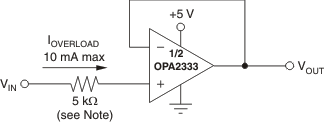
OPA2333-Q1 appin1_bos463.gif

NOTE:

A current-limiting resistor required if the input voltage exceeds the supply rails by ≥ 0.5 V.
Figure 18. Input Current Protection