SBOS463B December   2008  – February 2020 OPA2333-Q1

PRODUCTION DATA.  

  1. Features
  2. Applications
  3. Description
    1.     Device Images
      1.      0.1-Hz to 10-Hz Noise
  4. Revision History
  5. Pin Configuration and Functions
    1.     Pin Functions
  6. Specifications
    1. 6.1 Absolute Maximum Ratings
    2. 6.2 ESD Ratings
    3. 6.3 Recommended Operating Conditions
    4. 6.4 Thermal Information
    5. 6.5 Electrical Characteristics: VS = 1.8 V to 5.5 V
    6. 6.6 Typical Characteristics
  7. Detailed Description
    1. 7.1 Overview
    2. 7.2 Functional Block Diagram
    3. 7.3 Feature Description
      1. 7.3.1 Rail-to-Rail Input Voltage
      2. 7.3.2 Internal Offset Correction
    4. 7.4 Device Functional Modes
  8. Application and Implementation
    1. 8.1 Application Information
      1. 8.1.1 Achieving Output Swing to the Op Amp Negative Rail
    2. 8.2 Typical Application
      1. 8.2.1 High-Side Voltage-to-Current (V-I) Converter
        1. 8.2.1.1 Design Requirements
        2. 8.2.1.2 Detailed Design Procedure
        3. 8.2.1.3 Application Curve
        4. 8.2.1.4 Single Op Amp Bridge Amplifier
        5. 8.2.1.5 Low-Side Current Monitor
        6. 8.2.1.6 High-Side Current Monitor
        7. 8.2.1.7 Precision Instrumentation Amplifier
  9. Power Supply Recommendations
  10. 10Layout
    1. 10.1 Layout Guidelines
    2. 10.2 Layout Example
  11. 11Device and Documentation Support
    1. 11.1 Documentation Support
      1. 11.1.1 Related Documentation
    2. 11.2 Receiving Notification of Documentation Updates
    3. 11.3 Support Resources
    4. 11.4 Trademarks
    5. 11.5 Electrostatic Discharge Caution
    6. 11.6 Glossary
  12. 12Mechanical, Packaging, and Orderable Information

Package Options

Mechanical Data (Package|Pins)
Thermal pad, mechanical data (Package|Pins)
Orderable Information

Typical Characteristics

At TA = 25°C, VS = 5 V, and CL = 0 pF (unless otherwise noted)
OPA2333-Q1 typ1_bos463.gif
Figure 1. Offset Voltage Production Distribution
OPA2333-Q1 typ3_bos463.gif
Figure 3. Open-Loop Gain vs Frequency
OPA2333-Q1 typ5_bos463.gif
Figure 5. Power-Supply Rejection Range vs Frequency
OPA2333-Q1 typ7_bos463.gif
Figure 7. Input Bias Current vs Common-Mode Voltage
OPA2333-Q1 typ9_bos463.gif
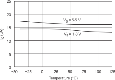
Figure 9. Quiescent Current vs Temperature
OPA2333-Q1 typ11_bos463.gif
Figure 11. Small-Signal Step Response
OPA2333-Q1 typ13_bos463.gif
Figure 13. Negative Over-Voltage Recovery
OPA2333-Q1 typ15_bos463.gif
Figure 15. Small-Signal Overshoot vs Load Capacitance
OPA2333-Q1 typ17_bos463.gif
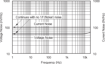
Figure 17. Current and Voltage Spectral Density vs Frequency
OPA2333-Q1 typ2_bos463.gif
Figure 2. Offset Voltage Drift Production Distribution
OPA2333-Q1 typ4_bos463.gif
Figure 4. Common-Mode Rejection Ratio vs Frequency
OPA2333-Q1 typ6_bos463.gif
Figure 6. Output Voltage Swing vs Output Current
OPA2333-Q1 typ8_bos463.gif
Figure 8. Input Bias Current vs Temperature
OPA2333-Q1 typ10_bos463.gif
Figure 10. Large-Signal Step Response
OPA2333-Q1 typ12_bos463.gif
Figure 12. Positive Over-Voltage Recovery
OPA2333-Q1 typ14_bos463.gif
Figure 14. Settling Time vs Closed-Loop Gain
OPA2333-Q1 typ16_bos463.gif
Figure 16. 0.1-Hz to 10-Hz Noise