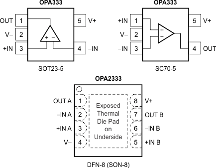
The OPAx333 series of CMOS operational amplifiers use a proprietary auto-calibration technique to simultaneously provide very low offset voltage (10 μV, maximum) and near-zero drift over time and temperature. These miniature, high-precision, low quiescent current amplifiers offer high-impedance inputs that have a common-mode range 100 mV beyond the rails, and rail-to-rail output that swings within 50 mV of the rails. Single or dual supplies as low as 1.8 V (±0.9 V) and up to 5.5 V (±2.75 V) can be used. These devices are optimized for low-voltage, single-supply operation.
The OPAx333 family offers excellent CMRR without the crossover associated with traditional complementary input stages. This design results in superior performance for driving analog-to-digital converters (ADCs) without degradation of differential linearity.
The OPA333 (single version) is available in the 5-pin SOT-23, SOT, and 8-pin SOIC packages, while the OPA2333 (dual version) is available in the 8-pin VSON, SOIC, and VSSOP packages. All versions are specified for operation from –40°C to 125°C.
PART NUMBER | PACKAGE | BODY SIZE (NOM) |
---|---|---|
OPA333 | SOT-23 (5) | 2.90 mm × 1.60 mm |
SOT (5) | 2.00 mm x 1.25 mm | |
SOIC (8) | 4.90 mm × 3.90 mm | |
OPA2333 | VSON (8) | 3.00 mm × 3.00 mm |
SOIC (8) | 4.90 mm × 3.90 mm | |
VSSOP (8) | 3.00 mm × 3.00 mm |
Changes from D Revision (November 2013) to E Revision
Changes from C Revision (May 2007) to D Revision
PIN | I/O | DESCRIPTION | |||
---|---|---|---|---|---|
NAME | SOIC | SOT | SC70 | ||
+IN | 3 | 3 | 1 | I | Noninverting input |
–IN | 2 | 4 | 3 | I | Inverting input |
NC | 1, 5, 8 | — | — | — | No internal connection (can be left floating) |
OUT | 6 | 1 | 4 | O | Output |
V+ | 7 | 5 | 5 | — | Positive (highest) power supply |
V– | 4 | 2 | 2 | — | Negative (lowest) power supply |
PIN | I/O | DESCRIPTION | ||
---|---|---|---|---|
NAME | VSON | SOIC, VSSOP | ||
+IN | — | — | I | Noninverting input |
+IN A | 3 | 3 | I | Noninverting input, channel A |
+IN B | 5 | 5 | I | Noninverting input, channel B |
–IN | — | — | I | Inverting input |
–IN A | 2 | 2 | I | Inverting input, channel A |
–IN B | 6 | 6 | I | Inverting input, channel B |
OUT | — | — | O | Output |
OUT A | 1 | 1 | O | Output, channel A |
OUT B | 7 | 7 | O | Output, channel B |
V+ | 8 | 8 | — | Positive (highest) power supply |
V– | 4 | 4 | — | Negative (lowest) power supply |
MIN | MAX | UNIT | ||
---|---|---|---|---|
Voltage | Supply | 7 | V | |
Signal input terminals(2) | –0.3 | (V+) + 0.3 | ||
Current | Signal input terminals(2) | –1 | 1 | mA |
Output short-circuit(3) | Continuous | |||
Operating junction temperature, TJ | 150 | °C | ||
Operating temperature, TA | –40 | 150 | ||
Storage temperature, Tstg | –65 | 150 |
VALUE | UNIT | |||
---|---|---|---|---|
V(ESD) | Electrostatic discharge | Human body model (HBM), per ANSI/ESDA/JEDEC JS-001(1) | ±4000 | V |
Charged-device model (CDM), per JEDEC specification JESD22-C101(2) | ±1000 |
MIN | MAX | UNIT | ||
---|---|---|---|---|
Supply voltage, VS | 1.8 | 5.5 | V | |
Specified temperature | –40 | 125 | °C |
THERMAL METRIC(1) | OPA333 | UNIT | |||
---|---|---|---|---|---|
D (SOIC) | DBV (SOT) | DCK (SC70) | |||
8 PINS | 5 PINS | 5 PINS | |||
RθJA | Junction-to-ambient thermal resistance | 140.1 | 220.8 | 298.4 | °C/W |
RθJC(top) | Junction-to-case (top) thermal resistance | 89.8 | 97.5 | 65.4 | °C/W |
RθJB | Junction-to-board thermal resistance | 80.6 | 61.7 | 97.1 | °C/W |
ψJT | Junction-to-top characterization parameter | 28.7 | 7.6 | 0.8 | °C/W |
ψJB | Junction-to-board characterization parameter | 80.1 | 61.1 | 95.5 | °C/W |
RθJC(bot) | Junction-to-case (bottom) thermal resistance | — | — | — | °C/W |
THERMAL METRIC(1) | OPA2333 | UNIT | |||
---|---|---|---|---|---|
D (SOIC) | DGK (VSSOP) | DRB (VSON) | |||
8 PINS | 8 PINS | 8 PINS | |||
RθJA | Junction-to-ambient thermal resistance | 124.0 | 180.3 | 46.7 | °C/W |
RθJC(top) | Junction-to-case (top) thermal resistance | 73.7 | 48.1 | 26.3 | °C/W |
RθJB | Junction-to-board thermal resistance | 64.4 | 100.9 | 22.2 | °C/W |
ψJT | Junction-to-top characterization parameter | 18.0 | 2.4 | 1.6 | °C/W |
ψJB | Junction-to-board characterization parameter | 63.9 | 99.3 | 22.3 | °C/W |
RθJC(bot) | Junction-to-case (bottom) thermal resistance | — | — | 10.3 | °C/W |
PARAMETER | TEST CONDITIONS | MIN | TYP | MAX | UNIT | |
---|---|---|---|---|---|---|
OFFSET VOLTAGE | ||||||
VOS | Input offset voltage | VS = 5 V | 2 | 10 | μV | |
dVOS/dT | Input offset voltage drift | TA = –40°C to 125°C | 0.02 | 0.05 | μV/°C | |
PSRR | Power-supply rejection ratio | VS = 1.8 V to 5.5 V, TA = –40°C to 125°C | 1 | 5 | μV/V | |
Long-term stability(1) | See note (1) | µV | ||||
Channel separation, dc | 0.1 | μV/V | ||||
INPUT BIAS CURRENT | ||||||
IB | Input bias current | TA= 25°C | ±70 | ±200 | pA | |
TA = –40°C to 125°C | ±150 | |||||
IOS | Input offset current | ±140 | ±400 | |||
NOISE | ||||||
Input voltage noise | f = 0.01 Hz to 1 Hz | 0.3 | μVPP | |||
f = 0.1 Hz to 10 Hz | 1.1 | |||||
in | Input current noise | f = 10 Hz | 100 | fA/√Hz | ||
INPUT VOLTAGE | ||||||
VCM | Common-mode voltage range | (V–) – 0.1 | (V+) + 0.1 | V | ||
CMRR | Common-mode rejection ratio | (V–) – 0.1 V < VCM < (V+) + 0.1 V, TA = –40°C to 125°C |
106 | 130 | dB | |
INPUT CAPACITANCE | ||||||
Differential | 2 | pF | ||||
Common-mode | 4 | pF | ||||
OPEN-LOOP GAIN | ||||||
AOL | Open-loop voltage gain | (V–) + 100 mV < VO < (V+) – 100 mV, RL = 10 kΩ, TA = –40°C to 125°C |
106 | 130 | dB | |
FREQUENCY RESPONSE | ||||||
GBW | Gain-bandwidth product | CL = 100 pF | 350 | kHz | ||
SR | Slew rate | G = +1 | 0.16 | V/μs | ||
OUTPUT | ||||||
Voltage output swing from rail | RL = 10 kΩ | 30 | 50 | mV | ||
RL = 10 kΩ, TA = –40°C to 125°C | 70 | |||||
ISC | Short-circuit current | ±5 | mA | |||
CL | Capacitive load drive | See Typical Characteristics | ||||
Open-loop output impedance | f = 350 kHz, IO = 0 A | 2 | kΩ | |||
POWER SUPPLY | ||||||
VS | Specified voltage range | 1.8 | 5.5 | V | ||
IQ | Quiescent current per amplifier | IO = 0 A | 17 | 25 | μA | |
TA = –40°C to 125°C | 28 | |||||
Turn-on time | VS = +5 V | 100 | μs | |||
TEMPERATURE | ||||||
TA | Specified range | –40 | 125 | °C | ||
Operating range | –40 | 150 | °C | |||
Tstg | Storage range | –65 | 150 | °C |
TITLE | FIGURE |
---|---|
Offset Voltage Production Distribution | Figure 1 |
Offset Voltage Drift Production Distribution | Figure 2 |
Open-Loop Gain vs Frequency | Figure 3 |
Common-Mode Rejection Ratio vs Frequency | Figure 4 |
Power-Supply Rejection Ratio vs Frequency | Figure 5 |
Output Voltage Swing vs Output Current | Figure 6 |
Input Bias Current vs Common-Mode Voltage | Figure 7 |
Input Bias Current vs Temperature | Figure 8 |
Quiescent Current vs Temperature | Figure 9 |
Large-Signal Step Response | Figure 10 |
Small-Signal Step Response | Figure 11 |
Positive Overvoltage Recovery | Figure 12 |
Negative Overvoltage Recovery | Figure 13 |
Settling Time vs Closed-Loop Gain | Figure 14 |
Small-Signal Overshoot vs Load Capacitance | Figure 15 |
0.1-Hz to 10-Hz Noise | Figure 16 |
Current and Voltage Noise Spectral Density vs Frequency | Figure 17 |
The OPAx333 is a family of Zero-Drift, low-power, rail-to-rail input and output operational amplifiers. These devices operate from 1.8 V to 5.5 V, are unity-gain stable, and are suitable for a wide range of general-purpose applications. The Zero-Drift architecture provides ultra low offset voltage and near-zero offset voltage drift.
The OPA333 and OPA2333 are unity-gain stable and free from unexpected output phase reversal. These devices use a proprietary auto-calibration technique to provide low offset voltage and very low drift over time and temperature. For lowest offset voltage and precision performance, optimize circuit layout and mechanical conditions. Avoid temperature gradients that create thermoelectric (Seebeck) effects in the thermocouple junctions formed from connecting dissimilar conductors. Cancel these thermally-generated potentials by assuring they are equal on both input terminals. Other layout and design considerations include:
Following these guidelines reduces the likelihood of junctions being at different temperatures, which can cause thermoelectric voltages of 0.1 μV/°C or higher, depending on materials used.
The OPA333 and OPA2333 operational amplifiers operate over a power-supply range of 1.8 V to 5.5 V (±0.9 V to ±2.75 V). Parameters that vary over supply voltage or temperature are shown in the Typical Characteristics section.
CAUTION
Supply voltages higher than +7 V (absolute maximum) can permanently damage the device.
The OPA333 and OPA2333 input common-mode voltage range extends 0.1 V beyond the supply rails. The OPA333 is designed to cover the full range without the troublesome transition region found in some other rail-to-rail amplifiers.
Typically, input bias current is approximately 70 pA; however, input voltages that exceed the power supplies can cause excessive current to flow into or out of the input pins. Momentary voltages greater than the power supply can be tolerated if the input current is limited to 10 mA. This limitation is easily accomplished with an input resistor, as shown in Figure 18.
The OPA333 and OPA2333 operational amplifiers use an auto-calibration technique with a time-continuous
350-kHz operational amplifier in the signal path. This amplifier is zero-corrected every 8 μs using a proprietary technique. Upon power up, the amplifier requires approximately 100 μs to achieve specified VOS accuracy. This design has no aliasing or flicker noise.
Some applications require output voltage swings from 0 V to a positive full-scale voltage (such as 2.5 V) with excellent accuracy. With most single-supply operational amplifiers, problems arise when the output signal approaches 0 V, near the lower output swing limit of a single-supply operational amplifier. A good, single-supply operational amplifier may swing close to single-supply ground, but does not reach ground. The output of the OPA333 and OPA2333 can be made to swing to, or slightly below, ground on a single-supply power source. This swing is achieved with the use of the use of another resistor and an additional, more negative power supply than the operational amplifier negative supply. A pulldown resistor can be connected between the output and the additional negative supply to pull the output down below the value that the output would otherwise achieve, as shown in Figure 19.
The OPA333 and OPA2333 have an output stage that allows the output voltage to be pulled to the negative supply rail, or slightly below, using the technique previously described. This technique only works with some types of output stages. The OPA333 and OPA2333 are characterized to perform with this technique; the recommended resistor value is approximately 20 kΩ.
NOTE
This configuration increases the current consumption by several hundreds of microamps.
Accuracy is excellent down to 0 V and as low as –2 mV. Limiting and nonlinearity occur below –2 mV, but excellent accuracy returns after the output is again driven above –2 mV. Lowering the resistance of the pulldown resistor allows the operational amplifier to swing even further below the negative rail. Resistances as low as 10 kΩ can be used to achieve excellent accuracy down to –10 mV.
The OPA2333 is offered in an DFN-8 package (also known as SON). The DFN is a QFN package with lead contacts on only two sides of the bottom of the package. This leadless package maximizes board space and enhances thermal and electrical characteristics through an exposed pad.
DFN packages are physically small, have a smaller routing area, improved thermal performance, and improved electrical parasitics. Additionally, the absence of external leads eliminates bent-lead issues.
The DFN package can be easily mounted using standard PCB assembly techniques. See Application Reports SLUA271, QFN/SON PCB Attachment and SCBA017, Quad Flatpack No-Lead Logic Packages, both are available for download at www.ti.com.
NOTE
The exposed leadframe die pad on the bottom of the package should be connected to V– or left unconnected.
The OPAx333 device has a single functional mode. The device is powered on as long as the power supply voltage is between 1.8 V (±0.9 V) and 5.5 V (±2.75 V).
NOTE
Information in the following applications sections is not part of the TI component specification, and TI does not warrant its accuracy or completeness. TI’s customers are responsible for determining suitability of components for their purposes. Customers should validate and test their design implementation to confirm system functionality.
The OPAx333 family is a unity-gain stable, precision operational amplifier with very low offset voltage drift; these devices are also free from output phase reversal. Applications with noisy or high-impedance power supplies require decoupling capacitors close to the device power-supply pins. In most cases, 0.1-μF capacitors are adequate.
The circuit shown in Figure 20 is a high-side voltage-to-current (V-I) converter. It translates in input voltage of 0 V to 2 V to and output current of 0 mA to 100 mA. Figure 21 shows the measured transfer function for this circuit. The low offset voltage and offset drift of the OPA333 facilitate excellent dc accuracy for the circuit.
The design requirements are as follows:
The V-I transfer function of the circuit is based on the relationship between the input voltage, VIN, and the three current sensing resistors, RS1, RS2, and RS3. The relationship between VIN and RS1 determines the current that flows through the first stage of the design. The current gain from the first stage to the second stage is based on the relationship between RS2 and RS3.
For a successful design, pay close attention to the dc characteristics of the operational amplifier chosen for the application. To meet the performance goals, this application benefits from an operational amplifier with low offset voltage, low temperature drift, and rail-to-rail output. The OPA2333 CMOS operational amplifier is a high-precision, 5-uV offset, 0.05-μV/°C drift amplifier optimized for low-voltage, single-supply operation with an output swing to within 50 mV of the positive rail. The OPA2333 family uses chopping techniques to provide low initial offset voltage and near-zero drift over time and temperature. Low offset voltage and low drift reduce the offset error in the system, making these devices appropriate for precise dc control. The rail-to-rail output stage of the OPA2333 ensures that the output swing of the operational amplifier is able to fully control the gate of the MOSFET devices within the supply rails.
A detailed error analysis, design procedure, and additional measured results are given in TIPD102.
The circuit shown in Figure 22 is a precision, low-level voltage-to-current (V-I) converter. The converter translates in input voltage of 0 V to 5 V and output current of 0 µA to 5 µA. Figure 23 shows the measured transfer function for this circuit. The low offset voltage and offset drift of the OPA333 facilitate excellent dc accuracy for the circuit. Figure 24 shows the calibrated error for the entire range of the circuit.
The design requirements are as follows:
The V-I transfer function of the circuit is based on the relationship between the input voltage, VIN, RSET, and the instrumentation amplifier (INA) gain. During operation, the input voltage divided by the INA gain appears across the set resistor in Equation 1:
The current through RSET must flow through the load, so IOUT is VSET / RSET. IOUT remains a well-regulated current as long as the total voltage across RSET and RLOAD does not violate the output limits of the operational amplifier or the input common-mode limits of the INA. The voltage across the set resistor (VSET) is the input voltage divided by the INA gain (that is, VSET = 1 V / 10 = 0.1 V). The current is determined by VSET and RSET shown in Equation 2:
A detailed error analysis, design procedure, and additional measured results are given in TIPD107.
The circuit shown in Figure 25 is a composite amplifier used to drive the reference on the ADS8881. The OPA333 provides excellent dc accuracy, and the THS4281 allows the output of the circuit to respond quickly to the transient current requirements of a typical SAR data converter reference input. The ADS8881 system was optimized for THD and achieved a measured performance of –110 dB. The linearity of the ADC is shown Figure 26.
The design requirements for this block design are:
The two primary design considerations to maximize the performance of a high-resolution SAR ADC are the input driver and the reference driver design. The circuit comprises the critical analog circuit blocks, the input driver, anti-aliasing filter, and the reference driver. Each analog circuit block should be carefully designed based on the ADC performance specifications in order to maximize the distortion and noise performance of the data acquisition system while consuming low power. The diagram includes the most important specifications for each individual analog block. This design systematically approaches the design of each analog circuit block to achieve a 16-bit, low-noise and low-distortion data acquisition system for a 10-kHz sinusoidal input signal. The first step in the design requires an understanding of the requirement of extremely low distortion input driver amplifier. This understanding helps in the decision of an appropriate input driver configuration and selection of an input amplifier to meet the system requirements. The next important step is the design of the anti-aliasing RC-filter to attenuate ADC kick-back noise while maintaining the amplifier stability. The final design challenge is to design a high-precision reference driver circuit, which would provide the required value VREF with low offset, drift, and noise contributions.
In designing a very low distortion data acquisition block, it is important to understand the sources of nonlinearity. Both the ADC and the input driver introduce nonlinearity in a data acquisition block. To achieve the lowest distortion, the input driver for a high-performance SAR ADC must have a distortion that is negligible against the ADC distortion. This parameter requires the input driver distortion to be 10 dB lower than the ADC THD. This stringent requirement ensures that overall THD of the system is not degraded by more than –0.5 dB.
It is therefore important to choose an amplifier that meets the above criteria to avoid the system THD from being limited by the input driver. The amplifier nonlinearity in a feedback system depends on the available loop gain. A detailed error analysis, design procedure, and additional measured results are given in TIPD115.
Figure 27 shows a temperature measurement application.
Figure 28 shows the basic configuration for a bridge amplifier.
A low-side current shunt monitor is shown in Figure 29. RN are operational resistors used to isolate the ADS1100 from the noise of the digital I2C bus. The ADS1100 is a 16-bit converter; therefore, a precise reference is essential for maximum accuracy. If absolute accuracy is not required and the 5-V power supply is sufficiently stable, the REF3130 can be omitted.
NOTE:
1% resistors provide adequate common-mode rejection at small ground-loop errors.Additional application ideas are shown in Figure 30 through Figure 33.
The OPAx333 is specified for operation from 1.8 V to 5.5 V (±0.9 V to ±2.75 V); many specifications apply from –40°C to 125°C. The Typical Characteristics presents parameters that can exhibit significant variance with regard to operating voltage or temperature.
CAUTION
Supply voltages larger than 7 V can permanently damage the device (see the Absolute Maximum Ratings).
TI recommends placing 0.1-μF bypass capacitors close to the power-supply pins to reduce errors coupling in from noisy or high-impedance power supplies. For more detailed information on bypass capacitor placement, refer to the Layout section.