SBOS233G March 2002 – April 2018 OPA2354 , OPA354 , OPA4354
PRODUCTION DATA.
- 1 Features
- 2 Applications
- 3 Description
- 4 Revision History
- 5 Device Comparison Table
- 6 Pin Configuration and Functions
- 7 Specifications
- 8 Detailed Description
- 9 Application and Implementation
- 10Power Supply Recommendations
- 11Layout
- 12Device and Documentation Support
- 13Mechanical, Packaging, and Orderable Information
Package Options
Mechanical Data (Package|Pins)
Thermal pad, mechanical data (Package|Pins)
- DDA|8
Orderable Information
8.3.8 Wideband Transimpedance Amplifier
Wide bandwidth, low input bias current, low input voltage, and current noise make the OPAx354 a preferred wideband photodiode transimpedance amplifier for low-voltage single-supply applications. Low-voltage noise is important because photodiode capacitance causes the effective noise gain of the circuit to increase at high frequency.
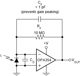
The key elements to a transimpedance design (as shown in Figure 36) are the expected diode capacitance [including the parasitic input common-mode and differential-mode input capacitance (2 + 2) pF for the OPAx354], the desired transimpedance gain (RF), and the gain-bandwidth product (GBW) for the OPAx354 (100 MHz, typical). With these three variables set, the feedback capacitor value (CF) may be set to control the frequency response.
 Figure 36. Transimpedance Amplifier
To achieve a maximally flat, second-order, Butterworth frequency response, the feedback pole must be set as shown in Equation 1:

Typical surface-mount resistors have a parasitic capacitance of approximately 0.2 pF that must be deducted from the calculated feedback capacitance value. Bandwidth is calculated by Equation 2:

For even higher transimpedance bandwidth, the high-speed CMOS OPA355 (200-MHz GBW) or the OPA655 (400-MHz GBW) may be used.